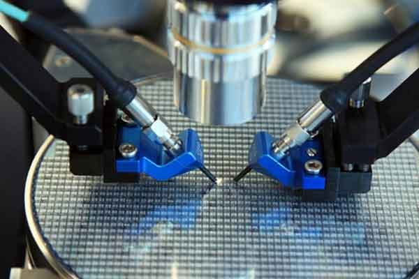
RF Test Probe
Precision Machined
CNCPioneer is a precision RF test probe manufacturer delivering controlled impedance coaxial RF probe components with tolerances as tight as ±0.003mm — 78+ Swiss CNC lathes, 66+ MAZAK mill-turn centers, GSG wafer probe tips, spring-loaded RF pogo pins, SMA through 1.0mm connector interfaces, and gold/rhodium plating.
What Is an
RF Test Probe?
An RF test probe is a precision-machined coaxial electrical contact assembly used to establish temporary, repeatable high-frequency electrical connections between a radio frequency test instrument — VNA, spectrum analyzer, signal generator, or RF power meter — and a device under test (DUT) at frequencies from DC through millimeter-wave bands above 110 GHz.
The fundamental technical challenge in RF test probe machining is maintaining controlled characteristic impedance — standardly 50Ω — from the probe body through the contact tip interface. At microwave and millimeter-wave frequencies, any dimensional deviation from the designed coaxial geometry creates an impedance discontinuity that generates signal reflections, degrades measurement accuracy, and limits the usable frequency range of the RF probe test solution.
-
50Ω impedance control Center conductor diameter ±0.003mm and outer conductor bore ±0.004mm maintains characteristic impedance within ±1Ω of 50Ω nominal — supporting DC to 110 GHz RF probe test applications.
-
GSG wafer probe precision GSG probe tip pitch accuracy ±3μm at 50μm pitch, tip height coplanarity ±5μm, tip radius ≤5μm — supporting on-wafer RF device characterization at the finest commercially available probe pitches.
-
TDR impedance verification Time domain reflectometry verification on assembled RF probe assemblies — characteristic impedance across probe body length, discontinuity identification at connector and tip transitions, ±1Ω specification.
-
40–60% China cost advantage China RF test probe machining delivers 40–60% cost reduction versus Japanese and US RF probe manufacturers — same coaxial geometry tolerances, impedance verification, and plating documentation.

Why CNCPioneer for
RF Test Probe Machining?
CNCPioneer offers Swiss CNC coaxial geometry precision, controlled impedance design understanding, and quality documentation that makes us a qualified supply partner for RF probe test solution developers, ATE equipment manufacturers, and microwave test instrument OEMs globally.
Coaxial Geometry for 50Ω
Center conductor diameter ±0.003mm and outer conductor bore ±0.004mm maintains the D/d ratio governing 50Ω characteristic impedance within ±1Ω — the fundamental precision requirement distinguishing RF test probe machining from standard connector manufacturing.
GSG Tip Geometry ±3μm
GSG probe tip pitch accuracy ±3μm for 50μm pitch assemblies, tip height coplanarity ±5μm, tip radius ≤5μm, and tip included angle ±0.5° — enabling on-wafer RF characterization at advanced node bond pad dimensions without adjacent pad shorting.
DC to 110 GHz Capability
SMA (26.5 GHz) through 1.0mm connector (110 GHz) coaxial interface components. Center conductor diameter of 0.122mm ±0.002mm for 1.0mm connector interfaces — at the boundary of standard precision machining capability, supported by CNCPioneer's Swiss CNC minimum-diameter machining.
Ra 0.2μm Signal Path Finish
Ra 0.2μm surface finish on all RF signal path surfaces — well below the skin depth at frequencies to 40 GHz — minimizes surface roughness conductor loss and ensures uniform gold plating distribution on center conductor and contact tip geometries.
TDR Impedance Verification
Characteristic impedance verified by TDR measurement on assembled RF probe assemblies — identifying discontinuities at connector interfaces and contact tip transitions, with impedance verification records included in the shipment documentation package.
40–60% China Cost Advantage
China RF test probe machining delivers 40–60% cost reduction versus Japanese and US RF probe manufacturers — same coaxial diameter tolerances, tip geometry accuracy, plating specifications, and TDR impedance documentation at significantly lower cost.
RF Test Probe Solutions
We Manufacture
CNCPioneer produces the complete range of RF test probe components — from coaxial RF probe bodies and GSG wafer probe tips to spring-loaded RF pogo pin assemblies, millimeter-wave connector interfaces, and calibration standard components — in brass, beryllium copper, tungsten, and specialty alloys with gold and rhodium plating.

Coaxial RF Test Probe Assemblies
50Ω and 75Ω coaxial RF test probe body, center conductor, and contact tip components from SMA (26.5 GHz) through 1.0mm connector (110 GHz). Center conductor diameter ±0.003mm, outer conductor bore ±0.004mm, coaxial concentricity ±0.003mm. TDR impedance verification on assembled components.

GSG Wafer Probe Tips
Ground-signal-ground probe tip assemblies for on-wafer RF and microwave device characterization. Pitch accuracy ±3μm for 50–250μm standard pitches, tip height coplanarity ±5μm, tip radius ≤5μm. GSGSG and multi-finger configurations for differential RF device characterization. Tungsten and beryllium copper tip materials.

Spring-Loaded RF Pogo Pins
Complete spring-loaded coaxial RF test probe assemblies — plunger, barrel, dielectric sleeve — for production test fixtures, burn-in sockets, and automated RF test handlers. BeCu plunger diameter ±0.003mm, barrel bore ±0.004mm, PTFE/PEEK dielectric sleeve for impedance control. TDR verification on assembled units.

SMA through 1.0mm Connector Interfaces
SMA (IEC 60169-15), SSMA, 2.92mm K-connector (40 GHz), 2.4mm (50 GHz), 1.85mm V-connector (67 GHz), and 1.0mm (110 GHz) interface body components. Thread pitch diameter ±0.005mm, pin diameter tolerances to ±0.002mm at sub-millimeter dimensions for millimeter-wave RF probe test solutions.

RF Calibration Standard Components
50Ω load standard body components with coaxial geometry machined to ±0.003mm for better than –50 dB return loss, calibration substrate interface components for SOLT and LRM calibration sequences, and impedance standard coaxial bodies for VNA RF probe test system calibration.

Custom & OEM RF Probe Components
Proprietary coaxial RF probe designs for non-standard impedances (75Ω, 93Ω, custom), novel contact geometries, differential/balanced probe configurations, and specialty RF probe test solution mechanical envelopes. DFM with coaxial impedance design review, prototype machining, TDR characterization, and complete qualification documentation.
Industries & Applications
CNCPioneer supplies RF test probe machining components to RF probe test solution developers, probe card manufacturers, ATE equipment OEMs, and microwave test instrument companies across semiconductor, wireless, automotive radar, aerospace, defense, and research industries worldwide.

Semiconductor Wafer Test
GSG probe tip components and coaxial RF test probe bodies for on-wafer RF and microwave device characterization in semiconductor R&D and wafer sort. Advanced node transistor S-parameter measurement, RF IC characterization, and millimeter-wave device measurement at 5G and beyond frequencies.

RF & Wireless Module Production Test
Spring-loaded coaxial RF pogo pin assemblies for automated production test of wireless LAN, Bluetooth, cellular, and satellite RF module products. High-throughput RF probe test solutions for smartphone RF front-end modules, Wi-Fi modules, and 5G mmWave module manufacturing test.

5G & Millimeter-Wave Test
High-frequency RF test probe components for 5G sub-6GHz and mmWave device characterization, 5G base station RF component test, and 24/28/39/60/77 GHz millimeter-wave radar module test. 1.85mm (67 GHz) and 1.0mm (110 GHz) connector interface components for mmWave probe test solutions.

Automotive Radar Test
Coaxial RF test probe solutions for 77 GHz automotive radar module characterization and production test. Automotive-grade RF probe components meeting IATF 16949 quality requirements for ADAS sensor and radar system supply chain qualification in automotive electronics manufacturing programs.

Aerospace, Defense & Satellite RF Test
High-reliability RF test probe components for satellite payload RF characterization, avionics RF module test, phased array antenna element measurement, and electronic warfare system characterization. AS9100D certified RF probe components for aerospace and defense RF test applications.

Research, Medical & Burn-In Test
Custom RF probe test solutions for university research, national laboratory characterization, and industrial R&D. Burn-in RF probe solutions with temperature-stable Kovar/Invar components and BeCu/Paliney contacts at 125–150°C. RF probe components for wireless medical device and implantable telemetry module test.
RF Test Probe Machining
Capabilities
CNCPioneer's Shenzhen facility combines 78+ Swiss CNC lathes for miniature center conductor elements, GSG probe tips, and coaxial body components with 66+ MAZAK mill-turn centers for larger RF probe body housings — with optical tip measurement, CMM verification, XRF plating inspection, and TDR impedance verification.
Swiss CNC Lathe Fleet
78+ Swiss CNC lathes (Star SR-32J, Citizen A20/A16, Tsugami B206, Nomura) · Center conductor Ø0.05mm minimum · Center conductor diameter ±0.003mm · Outer conductor bore ±0.004mm · Coaxial concentricity ±0.003mm · GSG pitch ±3μm · Tip angle ±0.5° · Ra 0.2μm signal path finish.
MAZAK Mill-Turn Fleet
66+ MAZAK mill-turn centers (Integrex, Quick Turn series) · Larger RF probe body housings · Probe station mounting and alignment structures · RF calibration fixture bodies · 5-axis simultaneous machining · Complex RF probe assembly housing geometry.
Coaxial Geometry Tolerances
50Ω: center conductor ±0.003mm, outer bore ±0.004mm → ±1Ω impedance · 75Ω configured on request · GSG pitch ±3μm · Tip height coplanarity ±5μm · Tip radius ±0.01mm · Thread pitch ±0.005mm · Surface finish Ra 0.2μm · TDR verified ±1Ω on assemblies.
Connector Interface Sizes
SMA — 26.5 GHz · SSMA — 40 GHz · 2.92mm K-connector — 40 GHz · 2.4mm — 50 GHz · 1.85mm V-connector — 67 GHz · 1.0mm — 110 GHz · All sizes machined with connector-specific interface gauge verification.
RF Signal Path Plating
Hard gold MIL-G-45204 Class 1 (0.5–1.5μm) for production RF fixtures · Soft gold for wafer probe card tips · Gold flash (0.05–0.1μm) for probe body conductors · Rhodium (HV 800–1000) for ultra-high cycle tips · Palladium-nickel HV 400–600 · Nickel underplate AMS 2403 — XRF verification every lot.
RF Probe Test Inspection
Mitutoyo CMM ±0.001mm — all coaxial dimensions · Optical microscopy — tip angle, radius, GSG pitch/coplanarity · Air gauge in-process diameter · XRF plating thickness per lot · TDR impedance verification on assembled probes · 100% optical tip inspection · Surface finish profilometry Ra 0.2μm.
RF Test Probe
Machining Materials
Material selection for RF test probe components balances electrical conductivity, mechanical spring properties, machinability precision, thermal stability, and plating compatibility for each probe element — from high-conductivity outer conductors to spring-loaded center conductor plungers and low-loss dielectric spacers.
C3604 (Free-Cutting)
Excellent machinability · Good conductivity · Cost-effective · RF probe body housings, outer conductor bodies, fixed contact probe components — primary RF probe body material
C2600 (Cartridge)
High ductility · Good conductivity · Coaxial body components requiring post-machining forming operations in RF probe body assembly
C17200 AT
Highest-strength copper alloy · Excellent spring properties · Good conductivity · Spring-loaded RF pogo pin plungers, cantilever probe tips, high-cycle coaxial probe contacts
C17500
High conductivity BeCu · Good spring properties · High-conductivity RF probe center conductor plungers requiring lower electrical resistance in the signal path
C51000
Good spring properties · Excellent corrosion resistance · Moderate-cycle RF probe spring contacts and secondary structural probe contact components
W / W-Ni
Extreme hardness · High wear resistance · Ultra-high cycle wafer probe card tips, wear-resistant contact tips for high-contact-count semiconductor RF probe test applications
WC-Co
Maximum hardness · Minimum tip wear · Long-life wafer probe tips for highest contact-count probe cards in production semiconductor RF wafer test programs
Kovar (ASTM F15) / Invar 36
Kovar: matched thermal expansion, good machinability · Invar 36: ultra-low thermal expansion · Temperature-stable RF probe housing components, burn-in RF probe assemblies, calibration reference components
PTFE / PEEK
PTFE: εr 2.1, excellent RF dielectric, chemical resistant · PEEK: εr 3.27, high mechanical strength · Coaxial dielectric spacers and RF probe body insulator components governing D/d ratio and impedance
Stainless 303 / 17-4PH / Ti Grade 5
Stainless: corrosion resistant structural components · Titanium: non-magnetic, lightweight · High-load alignment structures, probe station mounting hardware, magnetically sensitive RF measurement environments
Plating & Surface Finishing
for RF Test Probe Components
Surface plating on RF test probe components serves dual functions: electrical performance — providing low contact resistance, stable surface conductivity at microwave frequencies, and oxidation resistance — and mechanical performance — providing wear resistance on contact tip surfaces subject to repeated DUT touchdown cycles. Ra 0.2μm surface finish on all signal path surfaces ensures uniform plating distribution.
Hard Gold — MIL-G-45204 Class 1
Standard plating for RF test probe contact tips in ICT RF fixture, production test handler, and burn-in socket applications. Cobalt-hardened gold (HV 130–200) applied 0.5–1.5μm over nickel underplate. Stable low contact resistance, oxidation resistance, adequate wear resistance for hundreds of thousands of contact cycles. XRF thickness verification every production lot.
Soft Gold for Wafer Probe Tips
Pure soft gold (99.9% Au, HV 60–80) for wafer probe card RF tip components where maximum contact compliance and minimum contact resistance on delicate aluminum and copper bond pads are required. Soft gold's lower hardness reduces pad damage and maintains calibration stability across the probe card's operational life.
Gold Flash for RF Probe Body Components
Thin gold flash (0.05–0.1μm) over nickel underplate for RF probe body and outer conductor components where bulk conductivity and corrosion resistance are required without full precious metal cost. Gold flash prevents surface oxidation that would increase insertion loss at microwave frequencies where signal current flows only in the surface skin depth layer.
Rhodium Plating
Ultra-hard rhodium (HV 800–1000) for RF test probe contact tips in the highest-cycle RF probe test applications. Rhodium provides 5–10× longer contact tip life compared to hard gold in equivalent RF probe test applications, reducing probe replacement frequency in high-volume RF production test operations where probe replacement cost is a primary operational consideration.
Silver Plating for High-Power RF
High-conductivity silver plating for RF probe body inner surface conductors in high-power RF test probe applications. Silver's highest electrical conductivity of all metals (6.30×10⁷ S/m) minimizes insertion loss in RF probe body components at frequencies where conductor loss is the dominant signal path loss mechanism in power RF test applications.
Palladium-Nickel & Nickel Underplate
Palladium-nickel (80% Pd, 20% Ni, HV 400–600) as cost-effective hard plating for RF test probe contact tips requiring better cycle life than gold but lower cost than rhodium in moderate-cycle RF probe test fixture applications. Electroless nickel (AMS 2403) underplate beneath all gold, rhodium, and Pd-Ni on RF signal path surfaces for uniform thickness and diffusion barrier performance.
All RF test probe component plating certifications — XRF thickness records, plating adhesion verification, and visual inspection records — are provided with every shipment as part of the quality documentation package. TDR impedance verification records are included for all assembled RF test probe programs where impedance verification is specified.
Quality Assurance for
RF Test Probe Machining
RF test probe machining quality assurance extends beyond dimensional conformance to encompass coaxial geometry verification for impedance control, contact tip geometry optical measurement, Ra 0.2μm surface finish verification on signal path surfaces, XRF plating verification, and TDR characteristic impedance confirmation on assembled probes.
Material & Coaxial Design Review
Engineering review of RF test probe coaxial geometry impedance specifications, connector interface dimensional specs, contact tip geometry requirements, plating specifications, and frequency range performance requirements. Coaxial impedance design verification — D/d ratio calculation for target impedance and dielectric material — performed during DFM review.
RF Probe Machining Process Controls
Dedicated RF probe tooling with monitored wear limits; in-process center conductor diameter measurement by air gauge at defined intervals; coaxial concentricity verification after bore machining; contact tip geometry verification by optical measurement on first article and production samples; 100% optical tip geometry inspection.
First Article Dimensional Inspection
Complete Mitutoyo CMM dimensional report — center conductor diameter, outer conductor bore, coaxial concentricity, connector interface dimensions, contact tip geometry, and overall probe length. Optical tip radius and angle measurement. Surface finish Ra 0.2μm verification on all RF signal path surfaces. Balloon drawing referencing all drawing dimensions.
TDR Impedance Verification
TDR (time domain reflectometry) impedance verification on assembled RF test probe samples — characteristic impedance across probe body length, impedance discontinuity identification at connector interfaces and contact tip transitions. Impedance within ±1Ω of 50Ω nominal confirmed. TDR verification records included in shipment documentation package.
Plating & Contact Verification
XRF plating thickness measurement on gold, rhodium, and palladium-nickel plated RF probe contact components every production lot. Visual inspection under 10× magnification for plating uniformity on center conductor and contact tip surfaces. Contact resistance measurement at rated contact force for RF pogo pin assemblies. Spring force and over-travel verification.
Documentation Package
Material certifications with lot traceability; CMM dimensional reports; optical tip measurement records; surface finish records (Ra 0.2μm); XRF plating records; TDR impedance verification records; functional test records; and Certificate of Conformance — with every RF test probe machining shipment.
AS9100D & IATF 16949 Quality System
for RF Test Probe Machining
CNCPioneer's AS9100D and IATF 16949 dual-certified quality system meets the documentation and measurement requirements of RF probe test solution OEM qualification programs. We welcome on-site supplier qualification audits from RF test equipment OEM quality teams.
Coaxial Geometry Inspection
Complete CMM dimensional report — center conductor diameter, outer conductor bore, coaxial concentricity, connector interface geometry, and contact tip — with balloon drawing referencing all drawing dimensions. Coaxial D/d ratio verification confirming impedance compliance.
- Center conductor ±0.003mm verified
- Outer bore ±0.004mm, concentricity ±0.003mm
- Connector interface gauge verified
TDR Impedance Verification
TDR characteristic impedance measurement on assembled RF probe samples — impedance across probe body length within ±1Ω of 50Ω, discontinuity identification at connector and tip transitions. TDR verification records included in every RF probe assembly program shipment documentation.
- 50Ω ±1Ω TDR verified on assemblies
- Discontinuity identification at transitions
- TDR records in shipment documentation
Tip Geometry & Surface Finish
100% optical tip geometry inspection — angular accuracy ±0.5°, tip radius ±0.01mm, GSG pitch ±3μm, tip height coplanarity ±5μm. Ra 0.2μm surface finish verification on all RF signal path surfaces by contact profilometry. XRF plating thickness per lot.
- 100% optical tip geometry inspection
- Ra 0.2μm signal path finish verified
- XRF gold/rhodium plating every lot
OEM Documentation Package
Material certifications with lot traceability, CMM dimensional reports, optical tip measurement records, surface finish records, XRF plating records, TDR impedance verification records, functional test records (spring force, contact resistance), and Certificate of Conformance — structured for RF probe OEM qualification audit requirements.
- Certificate of Conformance (C of C)
- TDR impedance + CMM dimensional records
- AS9100D / IATF 16949 compatible
RF Test Probe FAQ
Common questions from RF probe test solution developers, probe card manufacturers, ATE equipment OEMs, and microwave test engineers about CNCPioneer's RF test probe machining capabilities and China RF test probe supply programs.
The ratio between center conductor outer diameter (d) and outer conductor bore diameter (D) is the most critical dimensional relationship for characteristic impedance control. For 50Ω PTFE-dielectric coaxial geometry, D/d must be maintained at 3.000 — a 1% error in either diameter produces approximately 0.5Ω impedance deviation. For a typical 50Ω RF pogo pin with a 1.0mm center conductor, center conductor diameter must be held to ±0.003mm and outer conductor bore to ±0.004mm to maintain characteristic impedance within ±1Ω of 50Ω nominal. These tolerances are tighter than standard connector manufacturing specifications and represent the fundamental technical challenge of RF test probe machining compared to general precision connector component production.
CNCPioneer's RF test probe machining supports components from DC through 110 GHz, limited by the coaxial connector interface size. SMA connector (3.5mm outer conductor): 26.5 GHz. 2.92mm K-connector: 40 GHz. 2.4mm: 50 GHz. 1.85mm V-connector: 67 GHz. 1.0mm: 110 GHz. For millimeter-wave frequencies above 110 GHz (WR-10, WR-8, WR-6 waveguide bands), we machine waveguide flange and transition components. The center conductor diameter of 0.122mm ±0.002mm required for 1.0mm connector components demonstrates our Swiss CNC lathe dimensional capability at the boundary of standard precision machining.
GSG probe pitch is the center-to-center distance between the signal tip and each adjacent ground tip. Standard GSG pitches for on-wafer RF measurement are 50μm, 100μm, 150μm, 200μm, and 250μm. Probe pitch is governed by the DUT pad layout — the on-wafer GSG contact pad structure must match the probe pitch within ±5μm for reliable landing on all three contact pads simultaneously. Finer probe pitch enables characterization of smaller, more densely integrated RF devices but requires tighter probe tip position accuracy and finer tip diameters to avoid adjacent pad shorting. CNCPioneer machines GSG probe tip components with pitch accuracy of ±3μm for 50μm pitch probe assemblies, supporting advanced node RF device characterization at the finest commercially available pitches.
For high-cycle spring-loaded coaxial RF test probe (RF pogo pin) plunger components requiring maximum contact cycle life above 500,000 cycles, we recommend beryllium copper C17200 AT condition with rhodium plating (HV 800–1000) on the contact tip. BeCu AT condition provides high yield strength (1170 MPa minimum), excellent spring-back maintaining consistent over-travel and contact force, and adequate electrical conductivity for RF signal transmission. Rhodium provides 5–10× longer contact tip life than gold. For moderate-cycle RF pogo pin applications below 200,000 cycles where cost is a consideration, brass C3604 plunger with hard gold plating provides acceptable performance. All BeCu RF test probe machining is performed with OSHA 29 CFR 1910.1024 compliant safety protocols.
Yes. CNCPioneer's RF test probe machining produces coaxial components for non-standard characteristic impedances including 75Ω (cable television and satellite broadcast), 93Ω (legacy computer networking), and custom impedances for particular transmission line environments. Custom impedance RF probe machining requires recalculation of the D/d coaxial geometry ratio for the target impedance and dielectric material, followed by verification that the resulting dimensions are achievable within our Swiss CNC lathe capability and maintain adequate mechanical integrity. Our engineering team performs impedance design review during DFM for all custom impedance RF test probe machining programs, providing calculated coaxial dimensions and dimensional tolerance analysis before prototype production.
Standard brass RF test probe body and outer conductor components without plating: 5–7 business days for prototype quantities. BeCu center conductor plunger components: 5–7 business days. Complete gold-plated RF pogo pin assemblies with TDR impedance verification: 10–14 business days for prototype quantities. GSG wafer probe tip components in tungsten or BeCu: 7–10 business days. Millimeter-wave RF test probe components in 1.0mm or 1.85mm connector sizes: 10–14 business days due to extended machining cycle times at sub-millimeter dimensions. Production quantities: 3–5 weeks depending on component complexity, material, and plating specifications.
CNCPioneer verifies characteristic impedance on assembled RF test probe components by TDR (time domain reflectometry) measurement using calibrated TDR equipment. TDR applies a fast-rise-time step signal to the probe input and measures the reflected signal as a function of time, converting time to distance along the probe transmission line and displaying impedance as a function of position from probe input to contact tip. TDR identifies impedance discontinuities at connector interfaces, dielectric transitions, and contact tip geometry changes, verifying that the machined coaxial dimensions produce the target characteristic impedance within ±1Ω specification. TDR verification records are included in the shipment documentation for all RF test probe assembly programs where impedance verification is specified.
CNCPioneer's China RF test probe machining price is typically 40–60% lower than equivalent components from established Japanese RF test probe manufacturers and 50–65% lower than US-based RF probe suppliers at comparable dimensional specification, plating, and TDR impedance documentation levels. The cost advantage reflects manufacturing economics rather than specification compromise — our RF probe components are machined to the same center conductor diameter tolerances, coaxial concentricity specifications, and Ra 0.2μm signal path surface finish requirements as leading Japanese and US RF probe manufacturers, verified by the same Mitutoyo CMM, optical tip measurement, and XRF plating equipment. Detailed OEM quotations are available within 24 hours.
Get a Quote for RF Test Probe Machining
Upload your RF test probe drawing, coaxial geometry specification, or RF probe test solution requirement and receive a free DFM review and competitive China RF test probe machining quotation within 24 hours. CNCPioneer's engineering team will review your probe design for machining feasibility, confirm coaxial geometry for target characteristic impedance, assess contact tip requirements for your DUT application, recommend optimal material and plating, and provide a complete OEM program quotation.