
Semiconductor
Test Probes
CNCPioneer machines wafer probe pins, IC socket probes, burn-in probes, power test probes and RF coaxial probe components with Swiss CNC accuracy, certified plating, optical inspection and production documentation.
What Are Semiconductor
Test Probes?
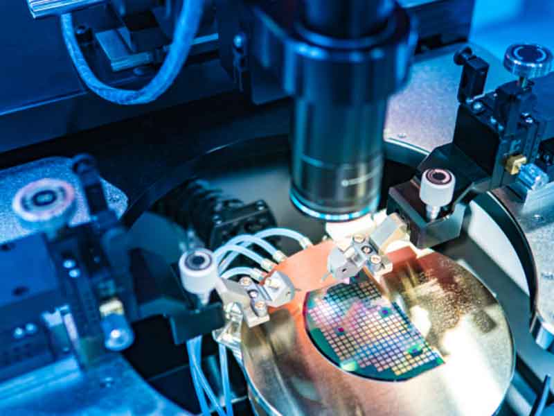
Semiconductor test probes create temporary electrical contact between ATE equipment and wafers, packaged ICs, sockets or power modules during production test and qualification.
The value of a probe is measured by repeatable contact: stable resistance, accurate tip geometry, consistent force, clean plating and predictable life across many touchdowns or insertion cycles.
-
±0.002mm shaft tolerance Swiss CNC machining supports fine shaft control, tip angle accuracy and repeatable guide-plate fit for wafer and socket probe applications.
-
Complete probe component range Vertical wafer pins, cantilever tips, BGA/LGA socket probes, burn-in probes, power probes, RF coaxial probes and probe-card hardware.
-
Tungsten and specialty alloy machining Dedicated processes for tungsten, rhenium-tungsten, BeCu, Paliney, Kovar, Invar, stainless steel and semiconductor-grade polymers.
-
Cost-effective China production Prototype and production programs can combine competitive machining cost with optical inspection, XRF plating records and clean packaging.

Why CNCPioneer for
Semiconductor Test Probes?
Probe performance depends on a tight combination of geometry, material, plating and inspection. CNCPioneer keeps those variables controlled from DFM through shipment documentation.
±0.002mm Shaft Tolerance
Swiss CNC guide-bushing support helps hold small probe shafts, tip geometry and concentricity for fine-pitch wafer cards and high-density socket contacts.
Tungsten Probe Machining
Dedicated tungsten and rhenium-tungsten machining protocols support vertical wafer probe pins, fine tips and high-wear contact components.
±5µm Tip Coplanarity
Controlled probe length and tip geometry help assembled arrays maintain uniform contact force across the full touchdown pattern.
High-Cycle Plating Options
Gold, rhodium, palladium-cobalt and silver plating options are selected by contact resistance, cycle life, temperature and current requirement.
RF Coaxial 50Ω Capability
Controlled center conductors, outer bores and dielectric interfaces support RF probe components with TDR verification when required.
China Cost Advantage
China-based Swiss CNC production helps reduce component cost while keeping optical inspection, plating verification and lot documentation in scope.
Types of Semiconductor
Test Probes We Manufacture
CNCPioneer produces probe pins, spring contacts, RF probe components and probe-card hardware for wafer sort, final test, burn-in, power device test and advanced packaging applications.

Vertical & Cantilever Wafer Probe Pins
Vertical, buckling beam and cantilever probe components for fine-pitch wafer cards, with tungsten, rhenium-tungsten, BeCu and palladium alloy options.

IC Socket Semiconductor Test Probes
BGA, LGA, QFP, flip-chip and CSP socket probe components with controlled plunger geometry, barrel bore accuracy and contact resistance.

Burn-In Socket Semiconductor Test Probes
High-temperature spring-loaded probe components for 125-150°C burn-in, using Paliney, Elgiloy, rhodium plating and thermally stable body materials.

Power Semiconductor Test Probes
Large-diameter force and sense probe components for MOSFET, IGBT, SiC and GaN device test, including low-resistance silver-plated contact designs.

RF Coaxial & GSG Semiconductor Test Probes
Coaxial, GSG and high-speed digital probe components for RF, mmWave and mixed-signal IC test, with impedance-sensitive features controlled by machining.

Probe Card Assembly Components
Guide plates, stiffener plates, space transformer hardware, socket housings and interface components for probe card and ATE socket assemblies.
Industries & Applications
We support probe card manufacturers, ATE socket suppliers and semiconductor test equipment OEMs across logic, memory, power, RF, automotive and advanced packaging test programs.

Logic & Memory Device Testing
Fine-pitch probe pins and high-density arrays for wafer sort and final test of logic, DRAM, NAND, SRAM and advanced node devices.

Power Semiconductor Device Testing
Low-resistance force and sense contacts for MOSFET, IGBT, SiC, GaN and power diode characterization and production test.

RF & Wireless IC Testing
Coaxial and GSG probe components for RF transceivers, Wi-Fi chipsets, 5G modem ICs, radar devices and mixed-signal test sockets.

Automotive-Grade IC Testing
Probe components for automotive MCUs, ADAS processors, power semiconductors and communication ICs with IATF-compatible documentation.

Advanced Packaging Test
Fine-pitch contacts and interface components for chiplets, HBM, SiP, FOWLP, 2.5D and 3D IC test sockets.

Burn-In & Reliability Qualification
High-temperature probe hardware for burn-in, reliability screening and qualification test where spring force and contact stability must hold over time.
Semiconductor Test Probes
Machining Capabilities
CNCPioneer's Shenzhen facility combines Swiss CNC, mill-turn machining, precious metal plating coordination and inspection records for miniature probe components and larger probe assembly hardware.
Swiss CNC Lathe Fleet
78+ Swiss CNC lathes for small shafts, plungers, probe pins and precision contact elements with tight diameter, length and concentricity control.
MAZAK Mill-Turn Fleet
66+ MAZAK mill-turn centers for probe card stiffeners, socket housings, guide plates, power probe barrels and complex interface hardware.
Probe Specifications
Support for shaft tolerance to ±0.002mm, tip coplanarity to ±5µm, RF 50Ω geometry and low-resistance power contact features.
Semiconductor Probe Materials
Tungsten, WC-Co, W-Re, BeCu, Paliney, Pd alloys, brass, stainless, Kovar, Invar, titanium, PEEK and ceramics with lot evidence.
Semiconductor Probe Plating
Hard gold, soft gold, rhodium, palladium-cobalt, silver and nickel underplate options selected by cycle life, current, temperature and contact material.
Semiconductor Test Probe Inspection
CMM, optical tip inspection, contact resistance checks, spring-force checks, TDR records for RF probes and XRF plating verification.
Materials for Semiconductor
Test Probes Machining
Material selection depends on wear, spring behavior, conductivity, temperature stability, dielectric isolation, plating compatibility and the expected number of test cycles.
W 99.95% Pure
Very hard probe material for wafer pins, cantilever tips and high-cycle applications where tip wear must be minimized.
WC-6% Co
Wear-resistant option for long-life cantilever tips and contact surfaces in high-touchdown wafer probe applications.
W-26% Re
Improved ductility versus pure tungsten for fine-pitch vertical probe pins and small-diameter wafer probe designs.
C17200 AT
High-strength spring material for IC socket plungers, burn-in contacts and high-cycle spring probe components.
Pd-Ag-Cu-Au-Pt-Zn
High-temperature spring alloy for burn-in socket probes where oxidation resistance and force retention matter.
Pd-Co / Pd-Ni
Spring-contact material for moderate-cycle wafer and socket probes where oxidation resistance supports stable contact.
C3604
Free-machining conductive material for barrels, housings and support components in probe and socket assemblies.
17-4PH
High-strength stainless for stiffeners, socket structural hardware and probe assembly components that need rigidity.
Kovar / Invar 36
Thermally stable materials for probe card stiffeners, ceramic-adjacent interfaces and burn-in hardware.
PEEK / Al2O3 / Si3N4 Ceramic
Insulating materials for guide plates, RF probe insulators, space transformer hardware and clean fixture components.
Titanium Grade 5 / C17500 BeCu
Titanium supports lightweight clean hardware; C17500 BeCu supports higher-conductivity power probe contacts.
Plating & Surface Finishing
for Semiconductor Test Probes
Plating is selected by pad material, contact force, current, cycle life, temperature and cleaning requirements. CNCPioneer can include XRF thickness records and contact-resistance evidence with the shipment package.
Hard Gold - MIL-G-45204 Class 1
Standard contact finish for IC socket and handler probes where stable resistance, moderate wear life and broad package compatibility are required.
Soft Gold for Wafer Probe Tips
Soft gold helps reduce pad damage on delicate aluminum, copper and bump contacts while maintaining low initial contact resistance.
Rhodium for High-Cycle Probes
Rhodium is used where tip wear and uptime are more important than lowest plating cost, especially in high-volume socket and fixture applications.
Palladium-Cobalt Plating
Pd-Co provides a middle ground between gold and rhodium for moderate-cycle probes that need better wear life and oxidation resistance.
Silver Plating for Power Semiconductor Test Probes
Silver supports high-current force contacts where low resistance and reduced heating are critical to accurate power device measurement.
Nickel Underplate & Gold Flash
Nickel underplate helps prevent base-metal diffusion beneath precious metal finishes; gold flash can protect non-contact body surfaces.
Plating records can include XRF thickness results, adhesion verification, visual inspection, contact resistance measurements and finish certificates by production lot.
Quality Assurance for
Semiconductor Test Probes
Probe quality control covers material verification, machining checks, optical tip inspection, functional testing, plating records, cleanliness and shipment documentation.
Material Incoming Inspection
Incoming lots are reviewed for alloy, condition, hardness, supplier certificate and traceability before probe machining begins.
Semiconductor Probe Machining Controls
Tooling, tool life, shaft diameter, length, tip geometry and clean handling are controlled during Swiss CNC and mill-turn operations.
Dimensional Inspection & Coplanarity
CMM and optical inspection can verify shaft diameter, concentricity, tip radius, angle, length and array coplanarity requirements.
Assembly Functional Testing
Contact resistance, spring force, over-travel, plunger motion and RF impedance can be checked according to the probe type and drawing.
Plating & Cleanliness Verification
XRF plating checks, visual inspection, ultrasonic cleaning, ESD-safe handling and ultra-clean packaging can be included when required.
Documentation Package
Release packages can include material certs, CMM reports, optical inspection records, XRF records, functional test data and C of C.
AS9100D & IATF 16949 Quality System
for Semiconductor Test Probes
CNCPioneer's quality system supports qualification needs for probe card manufacturers, ATE socket suppliers and semiconductor test equipment OEMs. Supplier audits are welcome.
100% Optical Tip Inspection
Optical inspection verifies tip shape, radius, angle and visible surface condition on probe contact features.
- Tip geometry inspection
- CMM shaft verification
- Array coplanarity support
Contact Resistance & Functional Testing
4-wire resistance, spring force, plunger movement and TDR checks can be applied according to probe type and qualification plan.
- Contact resistance testing
- Spring force measurement
- TDR for RF probes
XRF Plating & Material Traceability
XRF plating thickness records, material certificates, lot traceability and BeCu handling documentation can be included by order.
- XRF plating records
- Material lot traceability
- Certificate review
OEM Documentation Package
Documentation can include drawing-linked inspection, material evidence, plating records, functional test records and clean packaging notes.
- Certificate of Conformance
- CMM and optical records
- Ultra-clean packaging option
Semiconductor Test Probes FAQ
Short answers to common questions from probe card, socket and ATE equipment teams.
Vertical probes are arranged perpendicular to the wafer and are better for high-density, fine-pitch arrays. Cantilever probes bend from an angled beam and are simpler for standard-pitch wafer probing.
It depends on probe type, material, plating and contact force. IC socket probes are commonly verified by 4-wire resistance testing, while power probes use low-resistance force and sense designs for current-heavy measurements.
Concave cup tips are often used for BGA solder balls because they improve contact area and stability. The cup radius should match the ball size and insertion condition.
BeCu or Paliney with rhodium plating is often selected when cycle life and contact stability matter more than lowest material cost. The exact choice depends on temperature, force and contact material.
Shaft diameter, length, tip angle, tip radius, concentricity and guide-plate fit all matter because they affect contact location, force uniformity and coplanarity in the assembled array.
RF probe assemblies can be verified with TDR for impedance continuity. VNA S-parameter testing may be added when the program requires frequency-domain evidence.
Simple brass or BeCu prototype components can often be completed in about 5-7 business days. Tungsten, RF, plated or fully tested probe assemblies usually need more time.
The fair comparison is not price alone. Review machining tolerance, material traceability, optical inspection, plating verification, functional test evidence and qualification support. CNCPioneer combines those controls with China-based production economics.
Get a Quote for Semiconductor Test Probes
Upload your probe drawing, socket requirement or test application details. CNCPioneer will review machining feasibility, material, plating, inspection and packaging needs, then return DFM feedback and a quotation within 24 hours.