
Semiconductor
Probe Pin
CNCPioneer produces turned probe pins, spring probes, pogo contacts, wafer and package-test pins, IC socket contacts, burn-in pins, PCB probes, fixture pins, and custom micro-machined contacts. Swiss CNC turning, miniature-tip control, plunger-barrel fit, selective plating, low-burr finishing, and clean packaging support copper alloys, stainless, tool steel, and more. Qualified features reach ±0.005mm diameter and ±0.010mm concentricity; quotes arrive in 24 hours.

What Is a Semiconductor
Probe Pin?
A semiconductor probe pin connects a wafer, package, lead, pad, bump, coupon, or device to a test instrument or fixture. It may be a fixed micro-pin, spring probe, pogo contact, cantilever interface, socket contact, burn-in contact, or custom turned component. Its tip, force, travel, pitch, and resistance must suit the test surface and system.
Performance depends on tip geometry, diameter, straightness, hardness, force, stroke, overtravel, resistance, signal integrity, wear, contamination, and alignment. Before production, CNCPioneer aligns the probe and test interface with material, machining route, tip radius, plunger-barrel fit, finish, cleaning, inspection, and packaging.
-
Probe-pin DFM for tip, force, pitch, travel, and test surface We review wafer or package pad size, tip radius, pitch, force, stroke, overtravel, current, signal, wear, alignment, contamination risk, and replacement method before defining the machining route.
-
Swiss CNC turning for miniature pins, plungers, and barrels Guide-bushing Swiss CNC supports stable miniature tips and barrels. CNC turning and MAZAK mill-turn centres produce larger contacts, sockets, fixture bodies, and threaded probes.
-
Materials and finishes matched to stable electrical contact Copper alloys, brass, bronze, stainless, tool steel, and nickel alloys are matched to conductivity, spring force, wear, hardness, corrosion, and finish requirements.
-
24-hour quotes from a China precision factory Send a drawing, STEP file, pad data, tip profile, force, stroke, finish, cycle, and volume details. Quotes arrive within 24 hours, with DFM feedback in 48 hours.

Why CNCPioneer for
Semiconductor Probe Pins?
Our Swiss CNC and mill-turn platform combines conductive-alloy expertise, micro-tip and barrel DFM, force control, selective finishing, and clean packaging for semiconductor test programmes. China production can provide a 40–60% cost advantage.
Probe Tips for Wafer, Pad, Bump, and Package Tests
Probe tips must make reliable contact without damaging the wafer pad, bump, lead, or coupon. We review profile, radius, crown, chisel, flat, cup, point, contact area, pitch, alignment, force, travel, cleaning, and replacement needs. Tip geometry is controlled to the fixture and test surface.
Plunger, Barrel, and Spring-Probe Motion Control
Spring and pogo assemblies need a smooth plunger-barrel fit, stable spring seat, controlled stroke, and repeatable return. We review bore, diameter, guide length, spring rate, force, free length, travel, concentricity, wear, operation mode, and fixture alignment. Qualified production can achieve ±0.005mm plunger or barrel capability with test-system-matched concentricity.
Wafer, Package, Burn-In, and IC Socket Tests
Our probes serve wafer, final-package, burn-in, IC socket, memory, power-device, handler, fixture, and production tests. We define the pin, barrel, plunger, and termination around interface, pitch, current, signal, cycle count, resistance, thermal condition, fixture plate, replacement, and clean handling.
Materials and Plating Matched to Conductivity and Wear
C14500 balances conductivity and machining; C17200 serves resilient contacts; C36000 enables economical probes and barrels; phosphor bronze supports spring behaviour; stainless and tool steel suit guide or wear parts; and nickel alloys serve demanding environments. We match material and finish to resistance, force, wear, hardness, corrosion, and cycles.
Gold, Nickel, and Clean Surface Support
Gold supports low-level signals and corrosion resistance; nickel provides a barrier and wear layer; silver serves high conductivity; and tin suits selected terminals. We define thickness, tip wear, resistance, masking, dimensional allowance, movement, particle control, cleaning, and packaging by zone.
Clean Packaging and Production Documentation
Programmes can include material and plating certificates, dimensional reports, specified force, stroke, or resistance records, RoHS/REACH, COC, PPAP, AS9102 FAIR, and lot traceability. Clean trays, tubes, sealed bags, compartments, and bar-coded labels protect probes and prevent mixed lots.
Semiconductor Probe Pin
Product Portfolio
We produce wafer and package-test pins, pogo plungers and barrels, spring contacts, IC socket pins, burn-in contacts, PCB pins, power-device probes, and custom machined components.
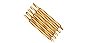
Wafer Test Probe Pins and Micro Contact Tips
Components for wafer probing, coupons, micro pads, bumps, and wafer-level fixtures. Point, crown, chisel, cup, ball, flat, and custom tips are available. DFM covers radius, diameter, pitch, force, travel, alignment, wear, and cleaning; materials and plating are matched to the application.
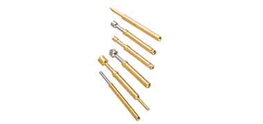
Package Test, IC Socket, and Burn-In Test Pins
Probe pins and socket contacts for final-package test, IC sockets, burn-in boards, memory test, power semiconductors, and device handlers. We control plunger diameter, barrel bore, spring seat, socket interface, depth, mating force, pitch, retention, finish, and thermal conditions around the socket and package.

Pogo Pins, Spring Probes, and Plunger-Barrel Assemblies
Spring-loaded assemblies with plungers, barrels, internal springs, tips, shoulders, flanges, and mounting features. DFM covers clearance, force, free length, stroke, overtravel, spring seat, return movement, resistance, cycle count, and clean assembly. Components can be supplied separately or as an approved assembly.
Industries & Applications
We support OEM programmes that need repeatable electrical contact, controlled force, low resistance, micro-tip geometry, clean handling, and traceable replacement components.

Wafer, Package & Burn-In Test
Probe pins for wafer, final-package, burn-in, memory, power-device, and automated-handler tests. DFM covers tip, pitch, pad or lead geometry, force, stroke, overtravel, current, signal, thermal condition, cycle count, replacement access, and clean handling.

Semiconductor Equipment & Wafer Handling
Probe pins, guide pins, spring contacts, fixture components, and sensor contacts for wafer handlers, test heads, alignment systems, and production tools. Miniature geometry, corrosion-resistant mechanical parts, gold or nickel plating, clean surfaces, low burrs, controlled force, and clean packaging are available.

IC Socket & Electronics Test Fixtures
Components for PCB inspection, IC sockets, ICT/FCT fixtures, continuity testing, validation, and handling. Low-force and high-cycle probes, fine pitch, gold plating, clean trays, specified force, stroke, or resistance records, and replacement identification are available.
Materials
Materials for
Semiconductor Probe Pins
Our material platform includes brass, high-conductivity and tellurium copper, beryllium copper, phosphor bronze, stainless, tool steel, nickel alloys, and customer-specified materials. Selection follows tip wear, force, conductivity, resistance, hardness, corrosion, plating, test cycles, and volume.
C36000 Free-Machining Brass
C36000 supports efficient production of probes, plungers, barrels, PCB contacts, and fixture components. It offers clean turning, stable dimensions, practical conductivity, and economical plating. We confirm tip geometry, plunger-barrel fit, spring seat, force, finish, burr control, wear, and cycle requirements before approval.
C11000 / C10200 Copper
C11000 or oxygen-free copper is selected for high-conductivity current paths and low resistance. We review machinability, tip and chip control, plunger contact, spring interface, finish, oxidation, heat, and storage protection. Solid or hollow tips, shoulders, barrels, and terminations are available.
C14500 Tellurium Copper
C14500 balances conductivity and machinability for probe pins, plungers, package contacts, and power-device interfaces. It supports complex small features with practical chip control. We review resistance, tip wear, finish, corrosion, heat, force, cycles, and dimensional stability.
C17200 Beryllium Copper
C17200 is suited to resilient plungers, spring contacts, high-cycle probes, and components requiring strength with conductivity. We define heat-treatment condition, machining sequence, hardness, force, finish, safety controls, and final inspection.
Phosphor Bronze and Special Copper Alloys
Phosphor bronze and special copper alloys serve spring interfaces, socket components, resilient contacts, low-friction parts, and corrosion-sensitive test components. Before quotation, we review conductivity, spring force, hardness, wear, cycles, finish, cleanability, safety, and availability.
303 / 304 / 316L Stainless and Tool Steel
Stainless supports corrosion-resistant barrels, guide sleeves, fixture parts, and mechanical probes; tool steel suits high-wear, high-cycle components. 303 prioritises machinability, 304 general corrosion resistance, and 316L demanding chemical or clean environments. Heat treatment, grinding, passivation, finish, and documentation are available for qualified programmes.
Surface Treatments for
Semiconductor Probe Pins
Finish selection follows contact resistance, tip wear, test cycles, force, signal stability, current, corrosion, particle control, and clean handling. We define thickness, masking, dimensional allowance, movement, contact-zone protection, cleaning, and post-finish inspection before production.
Gold Plating for Semiconductor Signal Probes
Gold can support low-level signal, wafer, package, and fine-pitch probes requiring stable contact and corrosion resistance. We define thickness, nickel underlayer, tip wear, force, cycles, selective plating, movement, contamination, and dimensional allowance.
Nickel Plating for Probe Barrel and Wear Protection
Nickel provides a barrier, corrosion protection, wear resistance, and a stable base for barrels, plungers, and mechanical zones. We review thickness, movement, resistance, spring seat, masking, diameter growth, particle control, and post-plate inspection. Selective nickel can protect guide and mounting surfaces.
Tin Plating for Power and Low-Resistance Probes
Tin can support power-test pins, battery probes, solderable terminations, and low-resistance interfaces. We review thickness, wear, movement, masking, dimensional allowance, specified storage requirements, and post-plate fit.
Silver Plating for High-Conductivity Probe Contacts
Silver is considered for high-conductivity probes, power-device tests, battery contacts, and specialised electrical fixtures. We review thickness, resistance, wear, anti-tarnish protection, selective plating, mating material, particle control, and packaging.
Low-Burr Deburring and Probe Cleaning
Probe pins need smooth tips, clean plungers, burr-free barrels, and unobstructed movement. The finishing plan can include precision deburring, brushing, washing, specified ultrasonic cleaning, drying, and visual inspection. Critical zones are protected through packaging.
Laser Marking and Clean Semiconductor Packaging
Part numbers, force codes, lot codes, orientation marks, clean trays, tubes, sealed bags, or compartments can protect tips and prevent mixed lots. We review mark location, readability, tip protection, particle control, traceability, and receiving labels for probe-card, socket, and fixture assembly.
Our DFM covers gold, nickel, tin, or silver plating; masking; deburring; cleaning; marking; specified force or resistance records; post-plate inspection; and clean packaging.
Quality System for
Semiconductor Probe Pins
Our IATF 16949 and AS9100D system controls four risks: tip, plunger, barrel, and material identity; force and stroke stability; plating and cleanliness; and traceable documentation. It supports wafer, package, burn-in, socket, fixture, and production tests.
Material, Tip, Spring, and Test-Surface DFM
Incoming brass, copper, stainless, tool steel, and special-alloy lots are checked against certificates and can receive alloy verification. DFM confirms pad or package interface, tip, pitch, force, stroke, spring seat, finish, cycles, current, signal, contamination risk, alignment, assembly, and inspection before machining.
- Material and certificate review for brass, copper, bronze, stainless, steel, nickel, and special alloys
- Tip, pad or lead geometry, pitch, force, stroke, overtravel, spring seat, and cycles reviewed
- Finish, masking, cleaning, dimensional allowance, and post-plate gauge plan defined
Swiss CNC and CNC Turning Tip / Barrel Control
Swiss CNC, CNC lathes, and MAZAK mill-turn centres are selected by probe diameter, tip, length, material, spring interface, test surface, volume, and tolerance. Small components are supported close to the cut; larger probes, threaded bodies, and fixture parts use stable datums. Capability can include ±0.005mm tip or barrel diameter, ±0.010mm concentricity, controlled tip radius, and repeatable spring seats.
- Swiss CNC for miniature wafer tips, package probes, pogo plungers, and barrels
- CNC turning and mill-turn for larger probes, fixture bodies, flanges, grooves, and threads
- Specified first-piece optical, CMM, pin-gauge, bore, stroke, and finish inspection
100% Critical Geometry and Post-Plating Inspection
Probes are inspected to drawing for tip, barrel, length, movement, spring seat, mounting features, concentricity, burrs, and finish. Specified post-plate checks cover thickness, tip area, appearance, dimensions, masking, movement, and mating fit. Force, stroke, resistance, cleanliness, particle control, and packaging can also be verified.
- 100% critical-dimension inspection for qualified programmes
- Specified post-plate diameter and contact-zone review
- Tip, movement, spring seat, burr, cleanliness, force, stroke, and finish inspection
Documentation — Reports, Certificates, PPAP, and FAIR
Available documents include dimensional reports, material and plating certificates, alloy verification, specified force, stroke, or resistance records, finish readings, RoHS/REACH, COC, PPAP Level 3, and AS9102 FAIR. Lot traceability links material, machining, plating, inspection, cleaning, and packaging records.
- Dimensional report, material certificate, plating certificate, and COC available
- PPAP Level 3 for automotive, EV, power semiconductor, and high-volume programmes
- AS9102 FAIR for aerospace, medical, semiconductor, and precision-equipment programmes
Semiconductor Probe Pin FAQ
Answers for equipment buyers and engineers on drawings, tip design, force, stroke, materials, plating, prototypes, and production lead times.
Send a 2D drawing or STEP file with probe function, pad geometry, tip, pitch, tip and barrel dimensions, material, force, stroke, spring specification, finish, resistance, cycles, quantity, and packaging. Without a drawing, a sample, fixture photos, pad or lead dimensions, current, and annual usage can support a quote.
Tip and force depend on pad or bump material, size, pitch, surface condition, acceptable marking, target resistance, cycles, alignment, and available travel. Point or crown tips can suit oxide-breaking or small pads, while flat, cup, ball, or chisel profiles may suit other surfaces. DFM reviews tip, force, stroke, spring rate, fixture tolerance, and wear before approval.
C36000 brass is common for plungers and barrels; C14500 and C11000 support conductivity; C17200 and phosphor bronze support resilient interfaces; and stainless or tool steel suits guide and wear parts. Gold serves signal contacts, nickel barrier and wear, silver high conductivity, and tin selected power or solderable interfaces. The right combination follows tip wear, force, resistance, cycles, cleanliness, and cost.
Simple turned probe components typically take 5–8 business days after drawing confirmation and material availability. Micro-tip, fine-pitch, spring-loaded, plated, force-tested, clean-packaged, or documentation-heavy programmes commonly take 8–15 days. Volume lead time depends on material, cycle time, supply, inspection, packaging, and quantity. Most inquiries receive a 24-hour quote and 48-hour DFM.
Get a Quote for Semiconductor Probe Pins
Upload a drawing or 3D model with pad or lead geometry, tip, force and stroke requirements, material and plating notes, test cycles, cleanliness needs, quantity, or annual usage. Receive a quote within 24 hours and DFM feedback within 48 hours.