Semiconductor
Test Probes
CNCPioneer is a precision semiconductor test probes manufacturer delivering high-reliability electrical contact components with tolerances as tight as ±0.002mm — 78+ Swiss CNC lathes, 66+ MAZAK mill-turn centers, gold, rhodium, palladium-cobalt, and silver plating, vertical wafer probes through power semiconductor test probes and RF coaxial probe assemblies.
What Are Semiconductor
Test Probes?
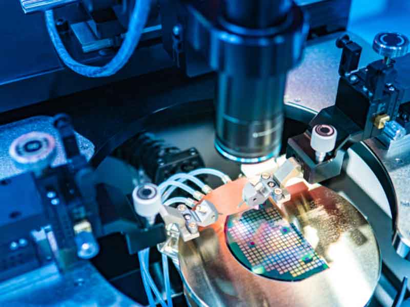
Semiconductor test probes are precision-machined electromechanical contact components that establish temporary, repeatable electrical connections between automated test equipment (ATE) and semiconductor devices — bare die at wafer level, packaged ICs in test sockets and handlers, and semiconductor modules in functional test fixtures — during manufacturing test, quality screening, reliability qualification, and failure analysis throughout the semiconductor production lifecycle.
The accuracy of semiconductor test probe contact directly determines the quality of semiconductor manufacturing test data. False failures from high contact resistance reject good devices and reduce yield; false passes from intermittent contact allow defective devices to reach customers. Both failure modes carry significant economic consequences in semiconductor manufacturing where test cost, yield, and quality are the primary profit drivers.
-
±0.002mm shaft tolerance Probe shaft diameter ±0.002mm and tip geometry angular accuracy ±0.3° for advanced wafer probe card applications — fine-pitch contact at 50μm pitch on 40×40μm bond pads without adjacent pad shorting.
-
Complete semiconductor probe range Vertical wafer probe pins (Ø25μm), cantilever probes, BGA/LGA/QFP IC socket probes, burn-in probes, power device probes (up to 200A), RF coaxial probes, and GSG wafer probe tips — all application types covered.
-
Tungsten & specialty alloy machining Dedicated tungsten probe machining protocols for vertical wafer probe pins. Paliney 7 for burn-in probes. Rhenium-tungsten for fine-pitch probes. BeCu C17200 AT for IC socket spring contacts — all materials with lot certifications.
-
40–60% China cost advantage China semiconductor test probes machining delivers 40–60% cost reduction versus Japanese and US probe suppliers — same ±0.002mm tolerances, 100% optical tip inspection, XRF plating documentation, and ultra-clean packaging.

Why CNCPioneer for
Semiconductor Test Probes?
CNCPioneer combines Swiss CNC sub-micron precision, semiconductor-grade precious metal plating, and quality documentation that makes us a qualified supply partner for probe card manufacturers, ATE socket suppliers, and semiconductor test equipment OEMs in the global semiconductor test probes market.
±0.002mm Shaft Tolerance
Swiss CNC lathe guide bushing support achieves probe shaft diameter tolerance of ±0.002mm and tip geometry angular accuracy of ±0.3° for fine-pitch wafer probe card applications — enabling reliable 50μm pitch contact on 40×40μm bond pads without adjacent pad shorting.
Tungsten Probe Machining
Dedicated tungsten probe machining protocols for vertical wafer probe pins in pure tungsten (HV 3000) and rhenium-tungsten alloy. Ø25μm minimum probe shaft diameter with Ra 0.2μm contact surface finish for uniform soft gold plating on wafer-level semiconductor test probes.
±5μm Tip Coplanarity
Probe pin length tolerance of ±0.010mm contributing to ±5μm tip coplanarity in assembled probe card arrays — the critical assembly-level specification ensuring uniform contact force across the full probe array at every wafer touchdown.
1M+ Cycle Rhodium Plating
Rhodium plating (HV 800–1000) for semiconductor test probes in the highest-cycle production test applications — 5–10× longer contact tip life than gold — directly reducing probe replacement frequency and ATE downtime in high-volume semiconductor manufacturing operations.
RF Coaxial 50Ω Capability
Center conductor diameter ±0.003mm and outer conductor bore ±0.004mm maintains 50Ω ±1Ω characteristic impedance with TDR verification for RF semiconductor test probes operating to 67 GHz in 5G, Wi-Fi 6/6E, and automotive radar IC production test.
40–60% China Cost Advantage
China semiconductor test probes machining delivers 40–60% cost reduction versus Japanese and US probe suppliers — same ±0.002mm tolerances, 100% optical tip inspection, XRF-verified plating, and ultra-clean packaging compatible with probe card assembly cleanroom environments.
Types of Semiconductor
Test Probes We Manufacture
CNCPioneer produces the complete range of semiconductor test probes — from vertical wafer probe pins and cantilever probe tips through IC socket spring probes, burn-in socket probes, power semiconductor test probes, RF coaxial probes, and probe card assembly components — in tungsten, beryllium copper, Paliney, and specialty alloys with certified precious metal plating.

Vertical & Cantilever Wafer Probe Pins
Vertical (buckling beam) probe pins at Ø25–150μm shaft diameter with ±0.002mm tolerance, ±0.3° tip geometry, ±5μm coplanarity for 50μm-pitch wafer probe cards. Cantilever probe pins at Ø50–250μm tip diameter for standard-pitch applications. Tungsten, rhenium-tungsten, BeCu, and Pd alloy materials. MEMS-compatible and cobra probe components.

IC Socket Semiconductor Test Probes
BGA socket probes with concave cup tip (±0.02mm radius matched to ball diameter), LGA socket probes with ±0.01mm height uniformity, QFP/gull-wing contact probes, and flip-chip/CSP probes at sub-100μm tip diameter. BeCu C17200 AT plungers with ±0.003mm barrel bore, contact resistance ≤20mΩ at rated force.

Burn-In Socket Semiconductor Test Probes
High-temperature spring-loaded probes for 125–150°C burn-in operations. Paliney 7 and Elgiloy plungers for high-temperature spring retention. Rhodium plating for contact resistance stability across thousands of thermal cycles. Kovar and Invar body components for thermally stable dimensional fit across burn-in temperature excursions.

Power Semiconductor Test Probes
Large-diameter spring-loaded probes for MOSFET, IGBT, SiC, and GaN power device final test carrying 10–200A. Contact resistance below 5mΩ for accurate RDS(on) measurement. Four-terminal Kelvin probe configurations with separate force and sense paths. Silver-plated copper alloy plungers (Ø2.0–8.0mm) for maximum current capacity.

RF Coaxial & GSG Semiconductor Test Probes
50Ω coaxial semiconductor test probes DC–67 GHz with TDR impedance verification ±1Ω. GSG wafer probe tip components at 50–250μm pitch with ±3μm accuracy and ±5μm coplanarity. High-speed digital probe components for >10 Gbps IC test. MIMO/phased array probe array components for 5G mmWave device characterization and AiP test.

Probe Card Assembly Components
Space transformer components (probe pad position ±5μm, flatness 0.01mm), probe head stiffener plates in Invar/stainless for thermal stability, guide plates in ceramic/metal (hole position ±3μm, bore ±0.002mm), probe card interface components, and final test handler socket contact components including Kelvin and high-temperature handler configurations.
Industries & Applications
CNCPioneer supplies semiconductor test probes to probe card manufacturers, ATE socket suppliers, and semiconductor test equipment OEMs serving logic, memory, power, RF/wireless, analog, automotive-grade, and advanced packaging semiconductor test applications worldwide.

Logic & Memory Device Testing
Semiconductor test probes for DRAM, NAND flash, SRAM, and logic IC production test at wafer sort and final test. High-density probe arrays for simultaneous multi-die testing on memory wafers. Fine-pitch wafer probe pins for advanced node logic die with copper bond pad pitch below 60μm at 7nm, 5nm, and 3nm technology nodes.

Power Semiconductor Device Testing
Semiconductor test probes for MOSFET, IGBT, SiC MOSFET, GaN HEMT, and power diode characterization and production test. Large-diameter power probes carrying drain currents of 10–200A with contact resistance below 5mΩ for accurate on-resistance measurement. Kelvin probe configurations for low-resistance power device parameter measurement.

RF & Wireless IC Testing
Semiconductor test probes for cellular RF transceivers, Wi-Fi 6/6E chipsets, 5G NR modem ICs, Bluetooth SoCs, and satellite communication ICs. Controlled impedance coaxial probes for RF signal path contact combined with high-density spring probes for DC power and digital signal access in mixed-signal IC test socket designs to 67 GHz.

Automotive-Grade IC Testing
Semiconductor test probes for automotive microcontrollers, ADAS processors, power semiconductors, and vehicle network communication ICs requiring AEC-Q100 qualification. High-temperature probes for burn-in at 150°C and cold temperature test at –40°C. IATF 16949 compatible documentation for automotive semiconductor supply chain compliance.

Advanced Packaging Test
Semiconductor test probes for 2.5D and 3D IC packages, chiplets with UCIe and HBM memory interfaces, fan-out wafer level packages (FOWLP), and system-in-package (SiP) modules. Fine-pitch probe arrays for sub-100μm bump pitch. Multi-die simultaneous contact for HBM memory stack characterization in advanced packaging test sockets.

Burn-In & Reliability Qualification
Burn-in semiconductor test probes for AEC-Q100 automotive IC qualification, MIL-SPEC defense IC screening, and commercial IC infant mortality elimination at 125–150°C over 24–168 hours. Paliney 7 and Elgiloy probes with rhodium plating for thermal cycling stability, combined with Kovar/Invar body components for dimensional stability across temperature excursions.
Semiconductor Test Probes
Machining Capabilities
CNCPioneer's Shenzhen facility combines 78+ Swiss CNC lathes for miniature vertical probe pins, cantilever probe tips, and IC socket plunger elements with 66+ MAZAK mill-turn centers for larger probe card components and power device test probe bodies — with 100% optical tip inspection, CMM verification, XRF plating, and TDR impedance verification.
Swiss CNC Lathe Fleet
78+ Swiss CNC lathes (Star SR-32J, Citizen A20/A16, Tsugami B206, Nomura) · Probe shaft Ø25μm minimum · Shaft diameter ±0.002mm · Tip geometry ±0.3° · Concentricity ±0.002mm · Probe length ±0.010mm · Tip coplanarity contribution ±5μm · Contact surface finish Ra 0.2μm · Dedicated tungsten machining protocols.
MAZAK Mill-Turn Fleet
66+ MAZAK mill-turn centers (Integrex, Quick Turn series) · Probe card stiffener plates · Space transformer metallic components · Power device test probe barrels (Ø2–8mm) · Guide plate machining · 5-axis simultaneous · Complex probe card interface and socket housing components.
Probe Specifications
Vertical probe shaft ±0.002mm · IC socket plunger/bore ±0.003mm · Tip geometry ±0.3° wafer / ±0.5° socket · Concave BGA tip radius ±0.02mm · GSG pitch ±3μm · Tip coplanarity ±5μm · Power probe contact resistance <5mΩ · RF coaxial 50Ω ±1Ω TDR verified · Guide plate hole ±0.002mm.
Semiconductor Probe Materials
Tungsten W 99.95% · Tungsten carbide WC-Co · Rhenium-tungsten W-26%Re · BeCu C17200 AT / C17500 · Paliney 7 · Pd-Co / Pd-Ni alloys · Brass C3604 · 17-4PH stainless · Kovar · Invar 36 · Ti Grade 5 · PEEK semiconductor grade · Al₂O₃ / Si₃N₄ ceramic — all with lot certifications.
Semiconductor Probe Plating
Hard gold MIL-G-45204 (0.5–2.0μm) · Soft gold (0.1–0.5μm wafer probes) · Gold flash (0.05–0.1μm body) · Rhodium HV 800–1000 (1M+ cycle) · Palladium-cobalt HV 400–600 · Silver ASTM B700 (power probes) · Nickel underplate AMS 2403 — XRF thickness verification every production lot.
Semiconductor Test Probe Inspection
Mitutoyo CMM ±0.001mm · 100% optical tip geometry inspection — angle ±0.3°, radius ±0.01mm · 4-wire contact resistance <20mΩ · Spring force ±10% calibrated gauge · TDR 50Ω ±1Ω RF probes · XRF plating per lot · Probe array coplanarity ±5μm CMM · Ultra-clean packaging for cleanroom probe card assembly.
Materials for Semiconductor
Test Probes Machining
Material selection for semiconductor test probes balances hardness and wear resistance for wafer-level probes, spring properties and conductivity for IC socket spring contacts, high-temperature stability for burn-in probes, and low resistance for power device test probes — with dedicated machining protocols for each material type.
W 99.95% Pure
Extreme hardness HV 3000 · High elastic modulus 411 GPa · Low deflection · Vertical wafer probe pins, cantilever probe tips, high-cycle wafer probe applications
WC-6% Co
Maximum hardness HV 1600 · Extreme wear resistance · Longest-life cantilever probe tips for highest-contact-count wafer probe applications
W-26% Re
Higher ductility than pure W · Good spring properties · Fine-pitch vertical probe pins, small-diameter wafer probe applications at sub-50μm pitch
C17200 AT
High yield strength 1170 MPa · Excellent spring properties · Good conductivity · IC socket probe plungers, burn-in probes, high-cycle spring contacts — 1,000,000+ cycle life
Pd-Ag-Cu-Au-Pt-Zn
Excellent high-temperature spring retention · Oxidation resistant · Burn-in socket probes, high-temperature semiconductor test at 125–150°C — premier burn-in probe material
Pd-Co / Pd-Ni
Good spring properties · Excellent oxidation resistance · Cantilever probe wires, moderate-cycle wafer probe applications where palladium oxidation resistance benefits contact stability
C3604
Excellent machinability · Good conductivity · IC socket barrel bodies, probe card housing components, and support hardware for semiconductor test probe assemblies
17-4PH
High strength · Good corrosion resistance · Probe card stiffener components, socket structural hardware, and high-load semiconductor test probe assembly components
Kovar / Invar 36
Kovar: matched CTE with ceramic, dimensionally stable · Invar 36: ultra-low thermal expansion · Space transformer interfaces, probe card stiffener plates, thermally stable burn-in socket components
PEEK / Al₂O₃ / Si₃N₄ Ceramic
PEEK: low outgassing, chemical resistant, good dielectric · Ceramic: dimensional stability, low CTE, electrical insulation · Guide plates, space transformer substrates, RF probe insulators
Titanium Grade 5 / C17500 BeCu
Titanium: lightweight, non-magnetic, cleanroom compatible · C17500: high-conductivity BeCu for power probe plungers requiring lower electrical resistance than C17200
Plating & Surface Finishing
for Semiconductor Test Probes
Gold is the universal contact surface material for semiconductor test probe tips, providing stable low contact resistance compatible with all semiconductor device terminal materials — aluminum bond pads, copper pillars, gold stud bumps, solder balls, and bare copper LGA pads. Ra 0.2μm contact surface finish on all probe tips ensures uniform precious metal plating distribution for consistent contact performance.
Hard Gold — MIL-G-45204 Class 1
Standard for IC socket and handler semiconductor test probes. Cobalt-hardened gold (HV 130–200), 0.5–2.0μm over 1.0–2.5μm nickel underplate. Compatible with BGA solder balls, LGA copper pads, QFP leads, and all standard IC package terminal materials. XRF thickness verification every production lot. Ideal for 100,000–500,000 cycle IC socket probe applications.
Soft Gold for Wafer Probe Tips
99.9% pure soft gold (HV 60–80), 0.1–0.5μm thickness for wafer-level semiconductor test probe tips contacting delicate aluminum and copper bond pads. Soft gold's lower hardness provides maximum contact compliance and minimum contact force, preventing pad damage and probe mark depth exceeding process specifications at advanced node die with copper pad dimensions below 30×30μm.
Rhodium — 1M+ Cycle Semiconductor Test Probes
Rhodium (HV 800–1000) for semiconductor test probes in the highest-cycle production test applications exceeding one million contact cycles — ICT fixture probes and final test handler socket contacts in high-volume semiconductor manufacturing. Rhodium provides 5–10× longer contact tip service life than gold, directly reducing probe replacement frequency and ATE downtime in high-throughput semiconductor test operations.
Palladium-Cobalt Plating
Palladium-cobalt (HV 400–600) for semiconductor test probe tips requiring better cycle life than gold at lower cost than rhodium. Good oxidation resistance and intermediate hardness for moderate-cycle semiconductor test socket and fixture probe applications — ATE socket probes at 100,000–500,000 cycle requirements where gold is insufficient but rhodium cost is not justified.
Silver Plating for Power Semiconductor Test Probes
High-conductivity silver plating for power semiconductor test probe plunger and contact surfaces carrying source/drain currents of 10–200A during MOSFET, IGBT, SiC, and GaN power device characterization. Silver's highest electrical conductivity of all metals minimizes resistive heating that corrupts device on-resistance (RDS(on)) measurements, enabling contact resistance below 5mΩ at rated current.
Nickel Underplate & Gold Flash
Electroless nickel underplate (AMS 2403) beneath all gold, rhodium, and palladium on semiconductor test probe contact surfaces — preventing base metal diffusion through precious metal layers that increases contact resistance over time, particularly critical at elevated temperatures in burn-in semiconductor test probe applications. Ultra-thin gold flash (0.05–0.1μm) for probe body and barrel oxidation protection without full contact plating cost.
All semiconductor test probes plating certifications — XRF thickness records per production lot, plating adhesion verification, visual inspection under 10× magnification for tip coverage uniformity, and contact resistance measurements on plated samples — are provided with every shipment supporting probe card manufacturer and ATE socket OEM qualification requirements.
Quality Assurance for
Semiconductor Test Probes
Semiconductor test probe quality assurance covers material qualification, 100% optical tip geometry inspection, coplanarity measurement for probe array assemblies, contact resistance and functional testing, XRF plating verification, ultra-clean packaging for cleanroom probe card assembly environments, and complete documentation supporting probe card manufacturer and ATE socket OEM qualification programs.
Material Incoming Inspection
Tungsten lot verification for purity (≥99.95% W) and hardness compliance; BeCu certification for C17200 AT hardness (HRC 38–43) and tensile strength; XRF composition verification on all materials; beryllium copper documentation per OSHA 29 CFR 1910.1024; Paliney 7 and specialty alloy certification with full compositional analysis and lot traceability.
Semiconductor Probe Machining Controls
Dedicated semiconductor probe tooling with monitored tool life limits; in-process probe shaft diameter measurement at defined intervals; tip geometry verification by optical measurement on first article and production samples; 100% optical inspection of probe tip geometry; ultra-clean handling protocols preventing probe tip contamination during machining operations.
Dimensional Inspection & Coplanarity
Complete Mitutoyo CMM dimensional report — probe shaft diameter ±0.002mm, tip geometry angular accuracy ±0.3°, probe length ±0.010mm, concentricity, and surface finish Ra 0.2μm on contact surfaces. Probe array coplanarity measurement to ±5μm specification for multi-pin wafer probe assemblies. Optical tip radius ±0.01mm and angle verification. Balloon drawing with full measurement results.
Assembly Functional Testing
4-wire Kelvin contact resistance measurement — <20mΩ IC socket probes, <5mΩ power device probes, <1Ω wafer probes at initial contact; spring force measurement within ±10% at rated compression; over-travel range verification; plunger sliding force compliance; TDR impedance verification 50Ω ±1Ω for RF semiconductor test probe assemblies.
Plating & Cleanliness Verification
XRF plating thickness measurement on gold, rhodium, palladium-cobalt, and silver plated semiconductor test probes every production lot. Visual inspection under 10× magnification for plating uniformity on probe tip surfaces. Ultrasonic cleaning; cleanroom inspection under particle-counting illumination; anti-static packaging for ESD-sensitive semiconductor test probe components; N₂-purged packaging available for ultra-clean probe card assembly environments.
Documentation Package
Material certifications with full lot traceability; CMM dimensional reports; 100% optical tip geometry records; surface finish records; XRF plating records; contact resistance and functional test records; TDR impedance records for RF probes; probe array coplanarity records; and Certificate of Conformance — with every semiconductor test probes shipment.
AS9100D & IATF 16949 Quality System
for Semiconductor Test Probes
CNCPioneer's AS9100D and IATF 16949 dual-certified quality system meets the documentation requirements of semiconductor test probes OEM qualification programs across probe card manufacturers, ATE socket suppliers, and semiconductor test equipment companies. We welcome on-site supplier qualification audits.
100% Optical Tip Inspection
100% optical tip geometry inspection on every semiconductor test probe — angular accuracy ±0.3° (wafer probes) / ±0.5° (socket probes), tip radius ±0.01mm, Ra 0.2μm surface finish. CMM probe shaft diameter ±0.002mm and concentricity ±0.002mm. Probe array coplanarity ±5μm for multi-pin assemblies.
- 100% optical tip geometry inspection
- CMM shaft ±0.002mm, concentricity verified
- Probe array coplanarity ±5μm CMM
Contact Resistance & Functional Testing
4-wire Kelvin contact resistance measurement — <20mΩ IC socket probes, <5mΩ power device probes at rated current, <1Ω wafer probes initial contact. TDR impedance 50Ω ±1Ω for RF probes. Spring force ±10% calibrated force gauge. Plunger sliding force compliance for stiction-free operation.
- <5mΩ power probes, <20mΩ socket probes
- TDR 50Ω ±1Ω RF probes verified
- Spring force ±10% calibrated gauge
XRF Plating & Material Traceability
XRF plating thickness measurement on gold, rhodium, palladium-cobalt, and silver plated semiconductor test probes every production lot. Tungsten purity (≥99.95% W) and BeCu AT condition hardness certified. Beryllium copper lot documentation per OSHA 29 CFR 1910.1024. Full material lot traceability from incoming bar stock to finished probe shipment.
- XRF plating thickness every production lot
- Tungsten purity ≥99.95% W certified
- BeCu AT condition hardness certified
OEM Documentation Package
Material certifications with lot traceability, CMM reports with balloon drawing, 100% optical tip geometry records, surface finish records, XRF plating records, contact resistance and functional test records, TDR impedance records for RF probes, and Certificate of Conformance. Ultra-clean N₂-purged packaging records for probe card assembly cleanroom environment compatibility.
- Certificate of Conformance (C of C)
- TDR records + CMM + optical tip geometry
- AS9100D / IATF 16949 / ultra-clean pkg
Semiconductor Test Probes FAQ
Common questions from probe card manufacturers, ATE socket suppliers, and semiconductor test equipment OEMs about CNCPioneer's semiconductor test probes machining capabilities and China semiconductor test probes supply programs.
Vertical probe pins stand perpendicular to the wafer surface and generate contact force through elastic buckling of the probe shaft under axial compression — the probe buckles laterally when compressed, generating predictable contact force governed by shaft diameter, length, material elastic modulus, and compression distance. Vertical probes enable the highest contact density and finest pitch capability (below 50μm) because probes can be packed closely in a two-dimensional grid without the clearance requirements of cantilever geometry. Cantilever probe pins extend at an angle from the probe card body and generate contact force through elastic bending of the probe wire during over-travel. Cantilever probes are simpler and less expensive but limited to pitch above 80μm and lower contact density, making them appropriate for standard-pitch device testing where the fine-pitch capability of vertical probes is not required.
Contact resistance in CNCPioneer's semiconductor test probe assemblies depends on probe type. For wafer-level vertical probe pins at initial contact: below 1Ω for tungsten probes with soft gold tip plating on aluminum bond pads. For IC socket spring-loaded semiconductor test probes at rated contact force: below 50mΩ standard, below 20mΩ for high-performance BeCu probes with optimized plating. For power semiconductor test probes at rated current: below 5mΩ using large-diameter silver-plated copper alloy probes for accurate RDS(on) measurement. For Kelvin four-terminal configurations requiring measurement accuracy below 1mΩ, we design separate force and sense current path probe configurations eliminating probe lead resistance from the measurement.
For BGA IC package semiconductor test probe contact, we recommend concave cup tip geometry with cup radius matched to 90–95% of the BGA solder ball radius. The concave cup maximizes contact area between probe tip and the spherical solder ball surface — instead of single-point contact from a flat or spear tip, the concave cup engages the ball across an annular contact zone providing lower and more consistent contact resistance. A cup that is too small contacts only the ball tip with minimal contact area; a cup that is too large contacts the ball equator and risks lateral ball displacement during socket insertion. CNCPioneer machines concave cup tip radius to ±0.02mm accuracy, and our engineering team recommends the appropriate cup radius for your specific BGA ball diameter and alloy during DFM review.
For semiconductor test probe applications requiring maximum contact cycle life above one million cycles, we recommend beryllium copper C17200 AT condition plunger material with rhodium plating (HV 800–1000) on the contact tip. BeCu AT condition provides spring-back properties and fatigue resistance maintaining consistent contact force across one million-plus compression cycles without spring force loss. Rhodium provides 5–10× longer contact tip life than gold in equivalent semiconductor test probe applications. For burn-in semiconductor test probes at 150°C requiring combined high-temperature spring retention and contact cycle life, Paliney 7 alloy plunger material with rhodium plating provides the optimal combination of high-temperature spring stability and contact surface durability. All BeCu machining is performed under OSHA 29 CFR 1910.1024 compliant beryllium safety protocols.
Fine-pitch wafer probe card semiconductor test probes at 50μm pitch require probe tip position accuracy of ±3μm to ensure reliable single-pad contact without adjacent pad shorting on bond pads as small as 30×30μm. Achieving ±3μm tip position accuracy in an assembled probe card requires probe shaft diameter tolerance of ±0.002mm to maintain consistent guide plate fit, probe length tolerance of ±0.010mm for coplanarity compliance, probe tip geometry angle accuracy of ±0.3° for consistent scrub mark direction, and guide plate hole position accuracy of ±2μm for probe tip position control. CNCPioneer's Swiss CNC lathe achieves probe shaft diameter tolerance of ±0.002mm and length tolerance of ±0.010mm for fine-pitch wafer probe specifications.
CNCPioneer verifies characteristic impedance in RF semiconductor test probe assemblies by TDR (time domain reflectometry) measurement using calibrated TDR equipment. TDR applies a fast-rise-time step signal to the probe RF input and measures the reflected signal as a function of time, displaying impedance versus position from probe input through contact tip. TDR identifies impedance discontinuities at connector interface transitions, dielectric material changes, and contact tip geometry changes, verifying that the machined coaxial dimensions produce 50Ω ±1Ω characteristic impedance across the probe body length. For RF semiconductor test probes in GSG wafer probe configurations, S-parameter measurement on a calibrated VNA verifies return loss and insertion loss versus frequency to the probe's rated upper frequency limit. TDR and S-parameter measurement records are included in the shipment documentation.
Standard material semiconductor test probes without plating — brass or BeCu IC socket probe components: 5–7 business days prototype quantities. Tungsten wafer probe pin components: 7–10 business days due to extended machining cycle times on tungsten. Gold-plated and rhodium-plated semiconductor test probe assemblies with contact resistance and functional testing: 10–14 business days prototype. RF coaxial semiconductor test probes with TDR impedance verification: 10–14 business days prototype. Production quantities: 3–5 weeks for standard configurations; 4–6 weeks for custom or specialty semiconductor test probe designs. Wholesale programs with blanket orders and scheduled delivery are available for probe card manufacturers and ATE socket OEMs requiring consistent large-volume supply.
CNCPioneer's China semiconductor test probes machining price is typically 40–60% lower than equivalent probes from established Japanese semiconductor test probe manufacturers. The cost advantage reflects manufacturing economics — lower labor cost, competitive material sourcing, and high-volume Swiss CNC machining efficiency — rather than specification compromise. Our semiconductor test probes are machined to the same probe shaft diameter tolerances, tip geometry accuracy, and coplanarity specifications as leading Japanese probe manufacturers, verified by the same Mitutoyo CMM, optical tip measurement, and XRF plating equipment. Ultra-clean packaging and complete documentation support probe card manufacturer and ATE socket OEM qualification requirements at significantly lower China probe component cost. Detailed OEM quotations are available within 24 hours.
Get a Quote for Semiconductor Test Probes
Upload your semiconductor test probe drawing, specification, or ATE socket design requirement and receive a free DFM review and competitive quotation within 24 hours. CNCPioneer's engineering team will review your probe design for machining feasibility, recommend optimal material and tip geometry for your semiconductor test application, confirm plating specification for required contact cycle life and resistance stability, and provide a complete OEM program quotation covering prototype, qualification, and volume production pricing.