
CNCPioneer is a certified precision manufacturer of stainless steel machining semiconductor parts delivering ultra-high purity components with tolerances to ±0.005mm and EP surface finish to Ra ≤ 0.25μm — 78+ Swiss CNC lathes, 66+ MAZAK mill-turn centers, in-house EP treatment, UHP cleaning, and cleanroom packaging.
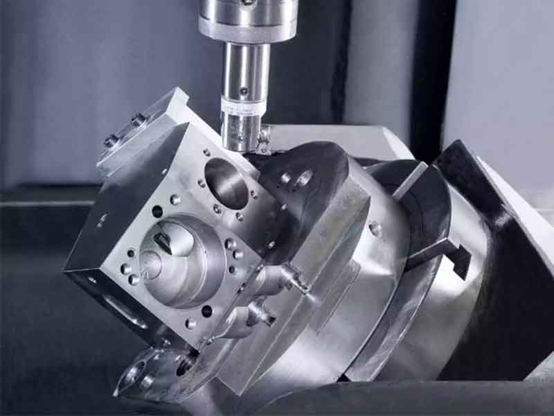
Stainless steel machining semiconductor parts are precision CNC-machined components produced from semiconductor-grade stainless steel alloys — primarily 316L VIM/VAR and 304L — for use in semiconductor wafer fabrication equipment, ultra-high purity gas delivery systems, vacuum process chambers, and metrology instruments. Stainless steel is the dominant material in semiconductor gas delivery because its combination of chemical inertness, EP treatability, and mechanical integrity at operating pressures makes it irreplaceable in UHP gas distribution, valve, fitting, and manifold applications.
The same 316L stainless steel used in standard industrial fittings becomes a fundamentally different product when processed as a stainless steel machining semiconductor part — subjected to VIM/VAR melting for ultra-low delta ferrite content, machined with dedicated semiconductor tooling, electropolished to TK EP grade Ra ≤ 0.25μm, passivated per ASTM A967, cleaned in ultra-pure deionized water, and packaged in ISO Class 5 cleanroom double-bag nitrogen-purged packaging.

CNCPioneer offers complete vertical integration — machining, EP surface treatment, UHP cleaning, and cleanroom packaging — in a single facility, delivering 316L VIM/VAR stainless steel machining semiconductor parts with the cleanliness, dimensional accuracy, and documentation that semiconductor equipment OEM qualification programs demand.
Mill certifications confirming delta ferrite content ≤1%, sulfur ≤0.005%, and alloy composition per ASTM A479 for every order — the mandatory material prerequisite for consistent TK EP grade surface finish on UHP gas delivery stainless steel parts.
TK EP grade (Ra ≤ 0.25μm) and BA grade (Ra ≤ 0.5μm) electrolytic polishing performed in-house at CNCPioneer's EP facility with controlled process parameters and Ra profilometry on every production batch — no outsourced EP lead time or documentation gaps.
Tooling, fixturing, and semiconductor-compatible cutting fluids with verified low metallic ion content are segregated from non-semiconductor machining operations — preventing cross-contamination that would compromise EP surface quality and final component cleanliness.
China-based precision manufacturing with in-house EP treatment, UHP cleaning, and cleanroom packaging delivers 30–50% cost reduction versus equivalent stainless steel machining semiconductor parts from Japanese, US, and European component suppliers — without compromising cleanliness or documentation.
316L SS without EP: 5–7 business days. With TK EP grade and UHP cleaning: 8–12 business days. Complex manifold stainless steel machining semiconductor parts with multiple VCR ports: 12–15 business days first article.
VIM/VAR material certs with heat number and delta ferrite records, CMM reports, EP process parameter records, cleanliness verification, and C of C — structured to support SEMI F19, F20, C78 compliance verification and OEM qualification audit requirements.
CNCPioneer produces the complete range of stainless steel machining semiconductor parts — from small-diameter VCR fittings and valve bodies to complex gas manifold blocks, vacuum chamber components, and wafer handling hardware — all with in-house EP treatment and UHP cleanroom packaging.

Straight, elbow, tee, cross, and reducing VCR fitting body, gland, and nut components in 316L VIM/VAR to SEMI C78 specifications. Face seal flatness 0.002mm, TK EP grade Ra ≤ 0.25μm, gland thread pitch diameter ±0.005mm. Complete EP process documentation included.

Diaphragm valve bodies, bellows valve bodies, and pneumatically actuated valve bodies for UHP semiconductor gas control. Gas-wetted EP finish Ra ≤ 0.25μm, valve seat Ra ≤ 0.2μm for bubble-tight shutoff, no dead volumes in internal flow path geometry.

Multi-port 316L VIM/VAR gas distribution manifold bodies with VCR port connections, valve mounting pads, and integrated flow paths. Port position accuracy ±0.02mm, all gas-wetted surfaces TK EP grade, no blind holes or dead leg volumes in internal geometry.

UHV ConFlat flange components with knife-edge geometry (tip radius 0.13mm ±0.025mm, Ra 0.4μm) to ANSI/AVS J1.4, plus ISO-K/ISO-F/KF vacuum flanges, vacuum chamber body components, and feedthrough shaft and housing assemblies.

Stainless steel chamber liner and shield components, showerhead assemblies (hole diameter ±0.01mm, position ±0.02mm), temperature control cooling block bodies, and pressure and flow sensor bodies — EP treated internal surfaces for minimal outgassing in semiconductor process environments.

Integrated gas stick bodies, mass flow controller flow tube bodies (orifice diameter ±0.005mm), pressure regulator body and poppet seat components (Ra ≤ 0.2μm), and tube fittings and adapters for stainless steel UHP semiconductor gas panel assemblies.
CNCPioneer supplies stainless steel machining semiconductor parts to semiconductor equipment OEMs, UHP gas system integrators, process chamber manufacturers, and vacuum equipment suppliers across the full semiconductor and adjacent equipment manufacturing spectrum.

VCR fittings, valve bodies, gas manifold blocks, gas stick components, and pressure regulator parts for ultra-high purity semiconductor process gas distribution — handling silane, arsine, phosphine, HF, chlorine, NF₃, and specialty dopant gases at purity levels to 6N.

Stainless steel machining semiconductor parts for chemical vapor deposition, atomic layer deposition, and physical vapor deposition process chamber hardware — showerhead assemblies, gas distribution components, chamber liners, and temperature control hardware.

ConFlat flange components, ISO and KF vacuum fittings, vacuum chamber body components, gate valve bodies, and feedthrough hardware for high-vacuum and ultra-high vacuum semiconductor process equipment and research instruments.

Stainless steel chamber liner and shield components, electrode and confinement ring support hardware, gas injection components, and process chamber structural elements for plasma etch, reactive ion etch, and ion implantation semiconductor process tools.

Stainless steel wrist shaft and joint components for atmospheric and vacuum wafer handling robots, FOUP opener interface hardware, cassette support elements, and kinematic mount components for 200mm and 300mm semiconductor fab AMHS systems.

Stainless steel machining semiconductor parts for MOCVD reactor gas delivery, MBE chamber hardware, and GaN, GaAs, SiC epitaxy equipment — plus solar cell manufacturing PECVD and wafer handling stainless steel components requiring semiconductor-grade cleanliness.
CNCPioneer's Shenzhen facility combines 78+ Swiss CNC lathes for small-diameter VCR fittings and valve components with 66+ MAZAK mill-turn centers for gas manifold blocks and vacuum chamber hardware — with complete in-house EP, passivation, UHP cleaning, and ISO Class 5 cleanroom packaging.
78+ Swiss CNC lathes (Star SR-32J, Citizen A20/A16, Tsugami B206, Nomura) · Ø0.5mm–Ø32mm · L/D up to 20:1 · OD tolerance ±0.005mm · Concentricity ±0.003mm · VCR face seal flatness 0.002mm · Bore surface finish Ra 0.4μm machined.
66+ MAZAK mill-turn centers (Integrex, Quick Turn series) · Ø10mm–Ø300mm · 5-axis simultaneous machining · Multi-port manifold bodies · Complex internal flow path geometry with no dead volumes · VCR port pattern accuracy ±0.02mm.
OD/bore ±0.005mm · VCR face flatness 0.002mm · Concentricity ±0.003mm · Port position ±0.02mm · Thread pitch diameter ±0.005mm · Knife-edge (CF) Ra 0.4μm · Perpendicularity 0.005mm · Internal bore Ra 0.4μm machined / Ra 0.25μm after EP.
316L VIM/VAR (delta ferrite ≤1%) · 304L VIM/VAR · 316L Standard · 304L Standard · 316L BA Tube interface fittings · 17-4PH for structural semiconductor parts · 440C for bearing applications — all with mill certifications and SII XRF incoming verification.
In-house TK EP grade (Ra ≤ 0.25μm) · BA grade (Ra ≤ 0.5μm) · ASTM A967 passivation · Mechanical polishing pre-treatment · High-P electroless nickel · EP process parameters controlled ±5% current density, ±2°C temperature, ±30 sec time — documented per batch.
Ultrasonic + megasonic cleaning in DI water (18.2 MΩ·cm) · IPA rinse & N₂ purge · Rinse water resistivity verification · Particle count per SEMI F20 · UV hydrocarbon inspection · Double-bagged N₂-purged packaging in ISO Class 5 cleanroom.
Stainless steel grade selection for semiconductor parts machining is governed by EP treatability, chemical compatibility with process gases and cleaning agents, mechanical strength at operating conditions, and weldability for fabricated semiconductor equipment assemblies. CNCPioneer stocks and machines all primary semiconductor stainless steel grades.
Delta ferrite ≤1% controlled · EP-compatible — TK EP grade achievable · UHP gas delivery, VCR fittings, valve bodies, gas manifolds
Delta ferrite 2–8% typical · Variable EP results · General semiconductor equipment, non-gas-wetted components, structural hardware
Delta ferrite ≤1% controlled · Excellent EP compatibility · Vacuum chamber components, structural semiconductor equipment, beam line hardware
Delta ferrite 2–5% typical · Good EP compatibility · Vacuum flanges, ISO fittings, general semiconductor structural components
Delta ferrite ≤1% · Pre-brightened · UHP gas distribution tubing interface fittings — bright annealed bore surface from tube manufacture
Martensitic · Not suitable for EP · High-strength structural semiconductor equipment shafts, actuator components, and high-load hardware
Martensitic · Not suitable for EP · High-hardness bearing components, valve poppet seats, and wear surfaces in semiconductor equipment
Electrolytic polishing is the most critical post-machining process for stainless steel machining semiconductor parts and the primary technical differentiator between semiconductor-grade and standard precision machined stainless steel. EP preferentially removes surface peaks, eliminates the work-hardened layer, and produces a chromium-enriched passive oxide surface — transforming as-machined Ra 0.8–1.6μm into TK EP grade Ra ≤ 0.25μm.
Standard finish for all gas-wetted stainless steel machining semiconductor parts. Preferential removal of surface peaks produces 5–10× roughness reduction from as-machined condition, eliminates embedded tool particles and free iron, and creates a chromium-enriched passive layer for minimum outgassing and particle generation. Full EP process documentation per SEMI F19 included.
Cost-effective EP option for stainless steel machining semiconductor parts requiring good surface cleanliness but not the extreme purity demands of process gas-wetted TK EP surfaces — vacuum system components, equipment enclosure hardware, and process chamber structural elements. Full Ra measurement documentation included.
Nitric acid passivation for stainless steel machining semiconductor parts requiring enhanced passive layer corrosion resistance without EP treatment. Removes free iron, enhances the chromium oxide passive layer, and improves chemical resistance to semiconductor process gases and cleaning agents. Standard for vacuum components, structural parts, and instrument bodies.
High-phosphorus electroless nickel (10–12% P) for stainless steel machining semiconductor parts requiring enhanced chemical resistance to aggressive semiconductor cleaning acids. Uniform coating thickness across complex manifold and valve body geometries. Applied over EP-treated base surfaces for maximum semiconductor equipment cleanliness compatibility.
Ultrasonic and megasonic cleaning in DI water (18.2 MΩ·cm), IPA rinse and nitrogen purge drying, particle count per SEMI F20, UV inspection for hydrocarbon contamination, and double-bagged nitrogen-purged packaging in ISO Class 5 cleanroom environment — standard for all stainless steel machining semiconductor parts.
Ra 0.4–0.8μm mechanical polishing as pre-EP surface preparation, improving EP treatment uniformity on complex geometries. Controlled uniform matte bead blasting as pre-passivation preparation for stainless steel semiconductor equipment structural components requiring non-reflective, uniform texture surfaces.
All stainless steel machining semiconductor parts surface treatment certifications — EP process records, passivation records, cleanliness verification, and SEMI standard compliance documentation — are provided with every shipment as part of the quality documentation package supporting semiconductor equipment OEM qualification requirements.
Quality assurance for stainless steel machining semiconductor parts extends beyond dimensional conformance to encompass 316L VIM/VAR material qualification, contamination control during machining, EP surface treatment verification, post-EP cleanliness validation, and the complete documentation trail required by semiconductor equipment OEM qualification programs.
316L VIM/VAR mill certification review confirming delta ferrite content ≤1%, sulfur ≤0.005%, alloy composition per ASTM A479, and heat number lot traceability. SII XRF composition verification on incoming bar stock. Material rejection for any lot failing delta ferrite or composition requirements.
Dedicated semiconductor tooling and fixturing segregated from non-semiconductor operations; semiconductor-compatible cutting fluids with verified low metallic ion content; inter-operation cleaning between machining stages; contamination-controlled handling with glove protocols throughout the stainless steel machining semiconductor parts production process.
Complete Mitutoyo CMM dimensional verification of all critical features — VCR face seal geometry, bore dimensions, port positions, thread form accuracy, and surface finish. Balloon drawing with full measurement results for semiconductor OEM first article qualification records.
Ra profilometry measurement on every production lot confirming TK EP (Ra ≤ 0.25μm) or BA grade (Ra ≤ 0.5μm) compliance. EP process parameter records (current density, electrolyte chemistry, temperature, time) retained per batch. Visual inspection in cleanroom lighting for EP surface uniformity and defects.
Ultrasonic cleaning in ultra-pure DI water (18.2 MΩ·cm); IPA rinse and nitrogen purge drying; rinse water resistivity measurement confirming cleaning agent removal; particle count verification by cleanroom optical inspection per SEMI F20 before double-bagged nitrogen-purged packaging.
316L VIM/VAR material certification with heat number and delta ferrite record; CMM dimensional report; Ra surface finish measurement records; EP process parameter records; post-EP cleaning records; particle count verification per SEMI F20; passivation records; and Certificate of Conformance with every shipment.
CNCPioneer's AS9100D and IATF 16949 certified quality system meets the material, surface treatment, and documentation requirements of semiconductor equipment OEM component qualification programs. We welcome on-site supplier qualification audits from semiconductor equipment OEM quality teams.
Complete CMM dimensional report with balloon drawing — VCR face seal geometry, bore dimensions, port positions, thread form, and surface finish — documented for semiconductor OEM first article qualification records.
Ra profilometry measurement confirming TK EP (Ra ≤ 0.25μm) per SEMI F19 on every production batch. EP process parameter records retained per lot. Visual cleanroom inspection post-EP for surface uniformity.
SII XRF verification on all incoming 316L VIM/VAR. Mill test reports with delta ferrite content (≤1%), sulfur content (≤0.005%), heat number, and lot number linked to every stainless steel machining semiconductor parts work order.
316L VIM/VAR material certification, CMM reports, EP process and Ra records, cleanliness verification (particle count, rinse water resistivity per SEMI F20), passivation records, and Certificate of Conformance — structured for SEMI F19/F20/C78 compliance and OEM qualification audit requirements.
Common questions from semiconductor equipment OEMs, UHP gas system integrators, and process chamber manufacturers about CNCPioneer's stainless steel machining semiconductor parts manufacturing and EP surface treatment capabilities.
316L VIM/VAR is required for UHP gas delivery stainless steel machining semiconductor parts because the VIM/VAR double-melting process produces controlled ultra-low delta ferrite content (≤1%) that is essential for achieving consistent TK EP grade surface finish. In standard 316L, delta ferrite content is typically 2–8% and randomly distributed in the microstructure. During EP treatment, the electrolyte preferentially attacks delta ferrite at higher dissolution rates than the austenitic matrix, creating micro-pits and surface roughness non-uniformity that makes TK EP grade Ra ≤ 0.25μm unachievable. 316L VIM/VAR with controlled delta ferrite ≤1% produces a uniform, all-austenitic microstructure that responds predictably and uniformly to EP treatment, enabling consistent TK EP grade surface finish across production lots.
TK EP grade (Ra ≤ 0.25μm / 10 μin) is the highest purity surface finish specification for gas-wetted stainless steel machining semiconductor parts in direct contact with ultra-pure semiconductor process gases — providing maximum particle generation reduction, minimum outgassing, and highest corrosion resistance for the most critical gas delivery applications including process gas distribution, valve bodies, and VCR fittings in contact with toxic and corrosive semiconductor gases. BA grade (Ra ≤ 0.5μm / 20 μin) is specified for general semiconductor equipment stainless steel components requiring good surface cleanliness but not the extreme purity demands of process gas-wetted surfaces — including vacuum system components, equipment enclosure hardware, and process chamber structural elements. CNCPioneer produces both TK EP and BA grade stainless steel machining semiconductor parts with full EP process documentation and Ra measurement verification on every production lot.
Yes. CNCPioneer designs and machines stainless steel gas manifold semiconductor parts with complex internal flow path geometry optimized to eliminate dead volumes, blind holes, and crevices that harbor process gas contamination and moisture in UHP semiconductor gas delivery systems. Our MAZAK mill-turn centers machine multi-port manifold bodies with intersecting flow path bores, precise port positioning, and smooth flow transition geometry in a single setup, eliminating assembly interfaces and mechanical joints that introduce dead volume and virtual leak risk. All internal gas-wetted surfaces are accessible for EP treatment and UHP cleaning in the finished manifold configuration.
CNCPioneer produces VCR face seal fitting stainless steel machining semiconductor parts in straight union, male connector, female connector, elbow (90° and 45°), tee, cross, reducing union, and bulkhead configurations to SEMI C78 and customer OEM dimensional specifications. All VCR fitting gas-wetted surfaces — face seal faces, internal bores, and flow path geometry — are EP treated to TK EP grade (Ra ≤ 0.25μm). VCR gland thread form accuracy is verified by calibrated thread gauges and CMM. Face seal flatness of 0.002mm is verified by Mitutoyo CMM on every first article and at defined production intervals. Material is 316L VIM/VAR with delta ferrite ≤1% certification included in the shipment documentation package.
Standard 316L stainless steel machining semiconductor parts without EP treatment: 5–7 business days for prototype quantities. With TK EP grade surface treatment and UHP cleaning: 8–12 business days for prototype quantities. Complex stainless steel gas manifold semiconductor parts with multiple VCR ports and EP treatment: 12–15 business days for first article quantities. Production quantities for standard VCR fittings and valve bodies: 3–4 weeks. Production quantities for complex manifold stainless steel machining semiconductor parts: 4–6 weeks. Long-term supply agreements with dedicated production capacity and committed lead times are available for semiconductor equipment OEM programs requiring consistent delivery schedules.
CNCPioneer provides a complete qualification documentation package including: 316L VIM/VAR material certification confirming alloy composition per ASTM A479, delta ferrite content (≤1%), sulfur content, and heat number lot traceability; CMM dimensional inspection report with balloon drawing referencing all critical features; Ra surface finish measurement records with profilometer trace data for all gas-wetted surfaces; EP process parameter records (current density, electrolyte chemistry, temperature, time) for each production batch; post-EP cleaning records including DI water resistivity measurements; particle count verification results per SEMI F20; passivation process records where applicable; and Certificate of Conformance. Documentation is structured to support SEMI F19, F20, and C78 standard compliance verification and semiconductor equipment OEM internal component qualification audit requirements.
CNCPioneer's contamination prevention program for stainless steel machining semiconductor parts includes: dedicated tooling used exclusively for semiconductor components to prevent cross-contamination from non-semiconductor materials; semiconductor-compatible cutting fluids with verified low metallic ion content and easy removal during post-machining cleaning; contamination-controlled handling with glove protocols throughout production; inter-operation cleaning between machining stages to remove chip and cutting fluid residue; post-machining ultrasonic cleaning in ultra-pure deionized water (18.2 MΩ·cm); post-EP cleaning with IPA rinse and nitrogen purge drying; particle count verification by cleanroom optical inspection per SEMI F20; and double-bagged nitrogen-purged packaging in ISO Class 5 cleanroom environment.
Stainless steel machining semiconductor parts are governed by SEMI F19 (specification for electrolytic passivation of metallic process-wetted components defining TK EP Ra ≤ 0.25μm and BA Ra ≤ 0.5μm grades), SEMI F20 (metallic contamination characterization of gas distribution system components), SEMI C78 (VCR face seal fitting dimensional specifications), and SEMI E49 (guide to semiconductor equipment installation). Material standards include ASTM A479 (stainless steel bars), ASTM A269 (seamless and welded austenitic SS tubing), and ASTM A967 (passivation treatments). Surface finish verification follows ASME B46.1 and ISO 4287. Vacuum component standards include ANSI/AVS J1.4 for ConFlat flanges and ISO 1609 for vacuum flanges.
Upload your semiconductor component drawing or CAD file and receive a free DFM review and competitive quotation within 24 hours. CNCPioneer's engineering team will review your component design for semiconductor stainless steel machining feasibility, confirm 316L VIM/VAR material compliance, assess EP grade surface treatment requirements, and provide a complete quotation covering machining, EP surface treatment, UHP cleaning, cleanroom packaging, and full semiconductor OEM documentation.