
Semiconductor CNC
Precision Machining
CNCPioneer is a certified semiconductor CNC machining manufacturer delivering ultra-precision components with tolerances as tight as ±0.005mm — 78+ Swiss CNC lathes, 66+ MAZAK mill-turn centers, EP surface treatment, UHP cleaning, and cleanroom packaging.
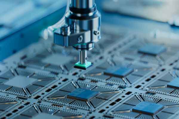
What Is Semiconductor
CNC Machining?
Semiconductor CNC machining is the precision manufacture of metallic and non-metallic components used in semiconductor wafer fabrication equipment, process chambers, gas delivery systems, vacuum systems, wafer handling automation, and metrology instruments. It demands the tightest dimensional tolerances, finest surface finishes, highest material purity standards, and most rigorous cleanliness requirements of any industrial machining application.
Contamination at the parts-per-billion level in semiconductor fabrication environments can destroy entire wafer lots worth millions of dollars. A single metallic particle or hydrocarbon trace on a gas-wetted component can introduce defects that reduce die yield or compromise process repeatability. Every dimension, surface finish, and material certification is a quality record supporting the equipment OEM's qualification program.
-
EP surface treatment specialist Electrolytic polishing to TK EP grade (Ra ≤ 0.25μm) for gas-wetted stainless steel components — the defining capability for UHP gas delivery system hardware.
-
316L VIM/VAR material expertise Semiconductor-grade 316L VIM/VAR, aluminum 6061, Inconel 625, Hastelloy C-276 — sourced with full material certifications confirming semiconductor industry cleanliness specifications.
-
Swiss + MAZAK dual capability Swiss CNC lathes for small-diameter VCR fittings, valve seats, and orifice components; MAZAK mill-turn centers for gas manifold bodies and process chamber hardware.
-
UHP cleanroom packaging Double-bagged, nitrogen-purged packaging in ISO Class 5 cleanroom environment. Full documentation: material certs, CMM reports, EP process records, cleanliness verification, and C of C.
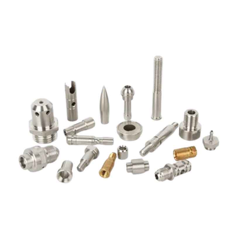
Why CNCPioneer for
Semiconductor CNC Machining?
CNCPioneer offers a combination of precision machining capability, surface treatment expertise, and contamination control protocols that make us a qualified supply partner for semiconductor equipment OEMs and process gas system integrators worldwide.
TK EP Surface Treatment
Electrolytic polishing to TK EP grade (Ra ≤ 0.25μm) on all gas-wetted surfaces. EP removes surface micro-roughness, embedded machining debris, and the work-hardened layer — producing the passive, chromium-rich oxide surface required for UHP gas delivery system components.
316L VIM/VAR Sourcing
Semiconductor-grade 316L VIM/VAR bar stock sourced with mill certifications confirming delta ferrite content compliance — the material prerequisite for consistent, defect-free EP surface treatment on gas delivery system components.
VCR Face Seal Precision
VCR fittings machined to face seal flatness of 0.002mm and face finish Ra 0.25μm (TK EP) — the surface quality required for reliable metal gasket seal integrity at operating pressures to 3,000 psi in UHP gas systems.
Cleanroom-Compatible Processing
Semiconductor CNC machining components processed, inspected, and packaged in contamination-controlled environments with double-bagged, nitrogen-purged packaging in ISO Class 5 cleanroom for ultra-high purity gas system components.
Significant Cost Advantage
China-based semiconductor CNC machining manufacturer cost structure delivers significant cost advantages over Japanese, European, and North American semiconductor equipment component suppliers without compromising surface cleanliness or dimensional accuracy.
Tier 1 Supply Experience
Established supply chain experience with demanding precision component programs including Hyundai Robot validates our process discipline for the dimensional and cleanliness requirements of semiconductor equipment OEM qualification programs.
Semiconductor CNC Machining
Components We Manufacture
CNCPioneer's CNC machining for semiconductor industry applications covers the complete range of precision components for front-end wafer fabrication equipment, back-end packaging equipment, and semiconductor metrology and inspection systems.

Gas Delivery System Components
VCR fittings and face seal components, UHP gas fittings, valve bodies, mass flow controller orifice components, and gas manifold blocks in 316L VIM/VAR with TK EP surface treatment (Ra ≤ 0.25μm) for ultra-high purity process gas systems.

Vacuum System Components
Vacuum chamber body components, ConFlat (CF) flanges with knife-edge geometry (Ra 0.4μm), vacuum feedthrough shaft and housing components, and turbomolecular pump rotor and stator components for high-vacuum and ultra-high vacuum semiconductor process equipment.

Wafer Handling & Transport Components
End effector blades with flatness 0.05mm and slot position ±0.02mm, wafer cassette and FOUP components, Bernoulli chuck gas distribution bodies, and aligner and centering components for 200mm and 300mm wafer handling robots.

Process Chamber Components
Showerhead and gas distribution plates (hole diameter ±0.01mm, pitch ±0.02mm), electrostatic chuck base plates, electrode and confinement ring components, and chamber liner and shield components for CVD, ALD, PVD, and plasma etch chambers.

Metrology & Inspection Equipment Components
High-accuracy linear and rotary stage components, optical system mounting hardware, probe card frame and stiffener components, and precision lens and mirror mount bodies for semiconductor wafer inspection and metrology instruments.

Valve, Regulator & Pressure Components
Diaphragm and bellows valve bodies, valve seat components (Ra 0.2μm), pressure regulator body and poppet components, and check valve hardware for semiconductor gas cabinet and process tool gas delivery and pressure control systems.
Industries & Applications
CNCPioneer supplies semiconductor CNC machining components to process equipment OEMs, gas system integrators, vacuum equipment suppliers, and wafer handling automation companies across the full spectrum of semiconductor and adjacent industries.

Front-End Wafer Fabrication
Semiconductor CNC machining components for CVD, ALD, PVD, plasma etch, ion implant, CMP, and photolithography process tools — process chamber hardware, gas delivery components, and vacuum system parts for leading-edge logic and memory fabrication.

Semiconductor Equipment OEMs
CNC machining for semiconductor industry equipment manufacturers including process tool OEMs, gas system integrators, vacuum equipment suppliers, and wafer handling automation companies. Qualified semiconductor CNC machining supplier supporting OEM component qualification programs.

Compound Semiconductor Manufacturing
Semiconductor CNC precision machining components for GaAs, GaN, InP, and SiC epitaxy and device fabrication equipment — MOCVD reactor components, MBE chamber hardware, and specialty gas delivery system parts.

Semiconductor Packaging Equipment
Back-end semiconductor packaging equipment components for wire bonding, flip-chip bonding, wafer-level packaging, FOWLP, and 3D IC stacking process tools requiring precision machined hardware with semiconductor-grade cleanliness.

Solar & Photovoltaic Manufacturing
Semiconductor CNC machining components for solar cell and photovoltaic module manufacturing equipment including PECVD deposition tools, screen printing equipment, and wafer handling systems for mono and polycrystalline silicon solar cell production.

Display & Metrology Equipment
CNC machining for flat panel display manufacturing equipment (LTPS TFT, OLED, microLED) and semiconductor metrology and inspection systems including CD-SEM, optical wafer inspection, and thin film metrology instrument components.
Semiconductor CNC Precision
Machining Capabilities
CNCPioneer's Shenzhen facility combines 78+ Swiss CNC lathes for small-diameter VCR fittings and valve components with 66+ MAZAK mill-turn centers for gas manifold blocks and process chamber hardware — with full EP, passivation, hard anodizing, and UHP cleaning capabilities.
Swiss CNC Lathe Fleet
78+ Swiss CNC lathes (Star SR-32J, Citizen A20/A16, Tsugami B206, Nomura) · Ø0.5mm–Ø32mm component diameter · Bore diameter to Ø0.5mm · L/D ratio up to 20:1 · OD tolerance ±0.005mm · Bore concentricity ±0.003mm · Surface finish Ra 0.4μm machined.
MAZAK Mill-Turn Fleet
66+ MAZAK mill-turn centers (Integrex, Quick Turn series) · Ø10mm–Ø300mm component diameter · 5-axis simultaneous machining · Multi-port manifold machining · Complex internal flow path geometry · VCR port pattern accuracy ±0.02mm · Deep bore capability.
Semiconductor Machining Tolerances
OD/bore diameter ±0.005mm · Concentricity ±0.003mm · Flatness (seal faces) 0.002mm · VCR face seal flatness 0.002mm · Surface finish Ra 0.25μm (TK EP) · Thread pitch diameter ±0.005mm · Angular port position ±0.1° · Perpendicularity 0.005mm.
Semiconductor Materials
316L VIM/VAR · 304L SS · Aluminum 6061-T6 / 2024 / MIC6 · Inconel 625 · Hastelloy C-276 · Titanium Grade 2 & 5 · PEEK (semiconductor grade) · PTFE (semiconductor grade) · Quartz / Fused Silica · Silicon (semiconductor grade) — full mill certifications.
EP & Surface Finishing
Electrolytic polishing TK EP grade (Ra ≤ 0.25μm) · BA grade (Ra ≤ 0.5μm) · ASTM A967 passivation · Type II & III hard anodizing · High-phosphorus electroless nickel · EP process records: current density, electrolyte chemistry, time, temperature retained per lot.
Ultra-High Purity Cleaning
Ultrasonic cleaning in DI water (18.2 MΩ·cm) · Megasonic cleaning · IPA rinse & N₂ purge drying · Particle count by cleanroom optical inspection · UV inspection for hydrocarbons · Double-bagged N₂-purged packaging in ISO Class 5 cleanroom.
Materials for Semiconductor
CNC Machining
Material selection for semiconductor CNC machining is governed by chemical compatibility with process gases and cleaning agents, outgassing performance in vacuum environments, surface treatability for EP and electropolishing, and contamination generation characteristics. CNCPioneer machines all primary semiconductor equipment materials with dedicated protocols.
316L VIM/VAR
Ultra-low carbon · Ultra-low delta ferrite · EP-compatible · VCR fittings, valve bodies, gas manifolds, UHP gas system components
304L
Low carbon · Good corrosion resistance · EP-compatible · General semiconductor equipment components, vacuum system hardware
6061-T6
Good machinability · Anodizable · Lightweight · Process chamber components, end effector blades, wafer handling hardware
2024-T351
High strength · Good machinability · Structural semiconductor equipment components and precision fixtures
MIC6 Cast Tooling Plate
Superior flatness · Stress-relieved · Precision fixture plates, electrostatic chuck base components, reference surfaces
PEEK (Semiconductor Grade)
Chemical resistant · Low outgassing · Radiolucent · Valve seat inserts, wafer contact components, electrical insulators
PTFE (Semiconductor Grade)
Chemically inert · Ultra-low outgassing · Valve seat components, gas line insulating fittings, seal elements
Inconel 625
Outstanding chemical resistance · High temperature · Corrosive gas system components, high-temperature process equipment
Hastelloy C-276
Outstanding pitting resistance in halogen environments · HF, Cl₂, and halide gas system components
Titanium Grade 2 / Grade 5
Excellent corrosion resistance · Lightweight · Corrosion-resistant semiconductor equipment structural components
Quartz / Fused Silica
Chemically pure · Low thermal expansion · UV transparent · Process chamber components, optical windows, electrode components
Surface Treatment for
Semiconductor CNC Machining Components
Surface treatment is the most critical post-machining process in semiconductor CNC precision machining. The as-machined surface is unacceptable for gas-wetted components — machining leaves surface micro-roughness, embedded tool particles, and hydrocarbon contamination that generate particles and outgas in semiconductor process environments.
Electrolytic Polishing (EP) — SEMI F19
The defining surface treatment for semiconductor gas delivery system components. EP preferentially removes surface peaks, producing a passive chromium-rich oxide layer with TK EP grade Ra ≤ 0.25μm and BA grade Ra ≤ 0.5μm. EP process controlled and documented with Ra measurement per batch and full process parameter records.
Passivation — ASTM A967
ASTM A967 and semiconductor industry specification compliant passivation for stainless steel semiconductor CNC machining components. Nitric acid passivation removes free iron and enhances the passive chromium oxide layer — improving corrosion resistance in aggressive process gas and cleaning chemical environments. Typically performed before EP treatment.
Hard Anodizing — Type II & Type III
Type III hard coat anodizing for aluminum semiconductor CNC machining components — hardness HV 400–600 for wear resistance, chemical resistance to semiconductor cleaning chemicals, and low particle generation for wafer contact applications. Precise thickness control (12–25μm) maintains dimensional accuracy after anodizing.
Electroless Nickel Plating
Uniform corrosion and chemical resistance coating for complex semiconductor equipment component geometries. High-phosphorus electroless nickel (10–12% P) provides maximum corrosion resistance in acidic semiconductor cleaning environments and uniform surface hardness across complex manifold and valve body geometries.
Ultra-High Purity Cleaning
Ultrasonic and megasonic cleaning in DI water (18.2 MΩ·cm), IPA rinse and nitrogen purge drying, particle count verification by cleanroom optical inspection, UV inspection for hydrocarbon contamination, and double-bagged nitrogen-purged packaging in ISO Class 5 cleanroom environment.
SEMI Standard Compliance Documentation
EP process records (current density, electrolyte chemistry, time, temperature) per SEMI F19 requirements, metallic contamination characterization per SEMI F20, cleanliness verification records, and Certificate of Conformance supporting semiconductor equipment OEM qualification programs and SEMI standard compliance verification.
Semiconductor CNC machining surface treatment certifications — including EP process records, passivation records, anodizing records, cleanliness verification, and SEMI standard compliance documentation — are provided with every shipment as part of the quality documentation package supporting semiconductor equipment OEM qualification requirements.
Quality Assurance for
Semiconductor CNC Machining
Semiconductor CNC machining quality requirements extend beyond dimensional conformance to encompass surface cleanliness, material purity, contamination control during processing, and the complete documentation trail required by semiconductor equipment OEM quality systems.
Contract & Drawing Review
Engineering review of semiconductor component drawing requirements, applicable SEMI standards, surface finish specifications (EP grade, BA grade), material purity requirements (316L VIM/VAR), and cleanliness requirements before order acceptance.
Material Incoming Inspection
SII XRF composition verification confirms 316L VIM/VAR alloy grade and delta ferrite content compliance; surface condition verification of incoming bar stock; mill test reports with heat number, lot traceability, and material certification retained for every semiconductor CNC machining order.
First Article Inspection
Complete CMM dimensional verification of all critical semiconductor component features including seal face geometry, bore dimensions, VCR port positions, and thread form accuracy — documented with balloon drawing and full measurement results for OEM qualification records.
Surface Treatment Verification
EP surface finish measurement by contact profilometry on every production batch; EP process parameter records (current density, electrolyte chemistry, time, temperature) retained per lot; visual inspection in cleanroom lighting for surface defects and contamination after EP treatment.
Cleanliness Verification
Post-cleaning particle count by cleanroom optical inspection; rinse water resistivity measurement confirming cleaning agent removal; visual inspection under UV illumination for hydrocarbon contamination — before double-bagged nitrogen-purged packaging in ISO Class 5 cleanroom.
Documentation Package
316L VIM/VAR material certifications with full heat traceability and delta ferrite records; CMM reports; EP surface finish measurement records with process parameters; cleanliness verification records; passivation and special process records; and Certificate of Conformance with every shipment.
AS9100D & IATF 16949 Quality System
for Semiconductor CNC Machining
CNCPioneer's AS9100D and IATF 16949 certified quality system meets the dimensional and documentation requirements of semiconductor equipment OEM qualification programs. We welcome on-site supplier qualification audits from semiconductor equipment OEM quality teams.
First Article Inspection
Complete CMM dimensional report with balloon drawing — seal face geometry, bore dimensions, port positions, VCR face flatness, and thread form accuracy documented for OEM qualification records. Surface finish measurement on all gas-wetted and process-wetted surfaces.
- Balloon drawing — all critical features
- CMM: seal faces, bores, port positions
- Material & EP process certifications
EP Surface Treatment Verification
Ra measurement by contact profilometry on every production batch confirming TK EP (Ra ≤ 0.25μm) or BA grade compliance. EP process parameter records (current density, electrolyte, time, temperature) retained per lot. Visual cleanroom inspection post-EP.
- Ra ≤ 0.25μm TK EP per batch
- EP process parameters retained per lot
- Cleanroom visual inspection post-EP
Material Traceability
SII XRF composition verification on all incoming 316L VIM/VAR bar stock. Mill test reports, heat numbers, and delta ferrite content records linked to every semiconductor CNC machining work order — unbroken traceability from mill certificate to finished component shipment.
- 316L VIM/VAR delta ferrite verified
- SII XRF alloy composition per lot
- Heat & lot number to work order linkage
OEM Documentation Package
Material certifications with full VIM/VAR traceability, CMM inspection reports, EP surface finish records, cleanliness verification records (particle count, rinse water resistivity), passivation process records, and Certificate of Conformance — formatted for SEMI standard compliance and OEM qualification audit requirements.
- Certificate of Conformance (C of C)
- EP records + cleanliness verification
- SEMI F19 / F20 compatible documentation
Semiconductor CNC Machining FAQ
Common questions from semiconductor equipment OEMs, process gas system integrators, and vacuum equipment suppliers about CNCPioneer's semiconductor CNC machining and semiconductor CNC precision machining capabilities.
EP (electrolytic polishing) grade surface finish in semiconductor CNC machining refers to the electrochemically polished surface condition required for gas-wetted stainless steel components in ultra-high purity gas delivery systems. The semiconductor industry defines two primary EP grades: TK EP grade with Ra ≤ 0.25μm (10 μin) for the most critical gas distribution system components in direct contact with ultra-pure process gases, and BA (bright annealed) grade with Ra ≤ 0.5μm (20 μin) for general semiconductor equipment applications. EP surface treatment is essential for semiconductor CNC machining components because it removes the mechanical work layer left by machining, produces a smooth, passive, chromium-rich oxide surface that minimizes particle generation and outgassing, and eliminates surface micro-crevices that harbor moisture and hydrocarbons incompatible with ultra-high purity semiconductor process environments.
316L VIM/VAR (vacuum induction melted / vacuum arc remelted) stainless steel is the semiconductor industry standard for UHP gas delivery system components machined by semiconductor CNC machining. The VIM/VAR processing produces ultra-low delta ferrite content (typically ≤ 1%), minimum non-metallic inclusion density, and highly uniform microstructure compared to standard 316L. Low delta ferrite content is critical because ferrite phase in austenitic stainless steel is preferentially attacked by the aggressive acids used in EP treatment, producing rough, inconsistent EP surfaces incompatible with semiconductor cleanliness requirements. CNCPioneer sources 316L VIM/VAR bar stock with mill certifications confirming delta ferrite content compliance for all semiconductor gas delivery system CNC machining orders.
CNCPioneer achieves VCR fitting face seal surface flatness of 0.002mm, face finish of Ra 0.25μm (TK EP grade) after electrolytic polishing, and gland thread pitch diameter tolerance of ±0.005mm for semiconductor CNC precision machining of VCR face seal fittings. These tolerances comply with SEMI C78 VCR fitting dimensional specifications governing metal gasket seating load and face seal integrity at operating pressures up to 3,000 psi. Face geometry and surface finish are verified by Mitutoyo CMM and contact profilometry on every first article and at defined production intervals, with results documented in the CMM inspection report accompanying each shipment.
CNCPioneer's contamination prevention program for semiconductor CNC machining includes: dedicated tooling used exclusively for semiconductor components to prevent cross-contamination from non-semiconductor materials; semiconductor-compatible cutting fluids verified for low metallic ion content and easy removal during post-machining cleaning; contamination-controlled handling with glove protocols throughout the machining process; inter-operation cleaning between machining stages to remove chip and cutting fluid residue; post-machining ultrasonic cleaning in ultra-pure deionized water; post-EP cleaning with IPA rinse and nitrogen purge drying; particle count verification by cleanroom optical inspection; and double-bagged nitrogen-purged packaging in ISO Class 5 cleanroom environment to maintain cleanliness through shipping and delivery.
Semiconductor CNC precision machining differs from standard industrial precision machining in five fundamental ways. First, dimensional tolerances are tighter — semiconductor gas fitting dimensions are typically held to ±0.005mm versus ±0.02mm for standard industrial components. Second, surface finish requirements are more demanding — TK EP grade Ra ≤ 0.25μm versus Ra 0.8–1.6μm for standard machined surfaces. Third, material specifications are more stringent — 316L VIM/VAR with controlled delta ferrite content versus standard 316L. Fourth, cleanliness requirements are categorically different — semiconductor CNC machining components must achieve particle counts and outgassing levels orders of magnitude below standard industrial components. Fifth, documentation requirements are more comprehensive — full material traceability, EP process records, surface finish measurement records, and cleanliness verification records are required for every semiconductor CNC machining lot.
For prototype quantities of standard semiconductor CNC machining components in 316L SS or aluminum 6061 without EP surface treatment, we deliver first article samples in 5–7 business days. Prototype components requiring EP surface treatment and UHP cleaning add 3–5 days for surface treatment processing, Ra measurement, and cleanroom packaging. Inconel and Hastelloy prototype semiconductor components require 10–14 days. Production quantities are completed in 3–5 weeks depending on component complexity, material, surface treatment requirements, and order volume. Long-term supply agreements with committed lead times are available for semiconductor equipment OEM programs requiring dedicated production capacity.
CNCPioneer supports compliance with SEMI F19 (specification for electrolytic passivation in semiconductor manufacturing equipment), SEMI F20 (metallic contamination characterization of gas distribution system components), SEMI C78 (VCR face seal fitting dimensions and tolerances), SEMI E1.9 (cassette specifications for 300mm wafer transport), SEMI E47.1 (FOUP mechanical specification for 300mm wafers), and SEMI F57 (polymer materials in ultrapure water and liquid chemical distribution). Surface finish verification per ASME B46.1 and ISO 4287, and material compliance per ASTM A479 and A269 are standard for semiconductor CNC machining components. Full documentation supporting SEMI standard compliance verification is included in the shipment documentation package.
Yes. CNCPioneer provides a complete semiconductor CNC machining documentation package supporting equipment OEM component qualification programs including: 316L VIM/VAR material certifications with full heat traceability and delta ferrite content records; CMM dimensional inspection reports with balloon drawings for all critical features; EP surface finish measurement records with Ra values and EP process parameter records; cleanliness verification records including particle count results and rinse water resistivity measurements; passivation process records; Certificate of Conformance; and first article inspection reports formatted per AS9102 for OEMs requiring formal FAIR documentation.
Get a Quote for Semiconductor CNC Machining
Upload your semiconductor component drawing or CAD file and receive a free DFM review and competitive semiconductor CNC machining supplier quotation within 24 hours. CNCPioneer's engineering team will review your component design for semiconductor CNC precision machining feasibility, confirm 316L VIM/VAR material compliance for gas delivery system applications, assess EP surface treatment requirements, and provide a complete quotation covering machining, surface treatment, cleaning, packaging, and documentation.