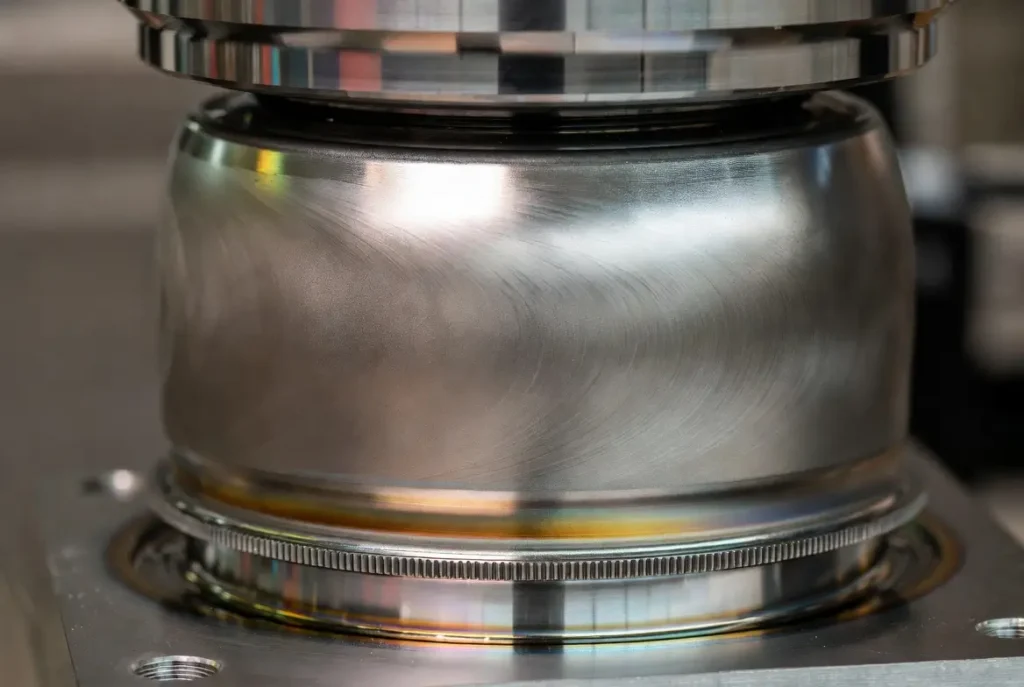
CNC machining for semiconductor industry plays a critical role in producing ultra precision semiconductor components used in advanced manufacturing systems.
As semiconductor devices continue to scale toward sub-10 nm and even angstrom-level architectures, the tolerance for mechanical deviation has reached unprecedented levels. In such environments, even a micron-level deviation in a structural component can lead to wafer misalignment, overlay errors, and ultimately yield loss.
Unlike traditional manufacturing sectors, semiconductor production demands a unique combination of:
- Ultra-high precision
- Extreme surface integrity
- Strict contamination control
- Thermal and structural stability
These requirements place CNC machining at the center of semiconductor equipment manufacturing.
Research in precision micro-manufacturing confirms that achieving stable machining at micro-scale requires coordinated control of tool dynamics, thermal effects, and machine kinematics [1]. Additionally, modern semiconductor equipment increasingly relies on ultra precision CNC machining to ensure repeatability and long-term stability across production cycles.
Quick Answer:
CNC machining in the semiconductor industry is used to manufacture ultra precision components such as wafer handling systems and vacuum chambers, ensuring high accuracy, stability, and contamination control.
What Is CNC Machining for Semiconductor Industry
CNC machining is a computer-controlled subtractive manufacturing process used to produce complex parts with high precision.
In semiconductor applications, CNC machining refers specifically to the fabrication of semiconductor CNC machining parts used in critical equipment such as lithography systems, etching chambers, and wafer transfer mechanisms.
Core Characteristics of Semiconductor CNC Machining
To meet industry requirements, CNC machining must achieve:
- Micron or sub-micron tolerances
- Ultra-smooth surface finishes (Ra < 0.4 µm)
- Minimal subsurface damage
- Cleanroom compatibility
Unlike standard machining, precision semiconductor components are highly sensitive to micro-scale variations. Factors such as tool vibration, thermal drift, and material anisotropy can significantly affect final accuracy[3].
Micro-Scale Machining Behavior
At micro-scale, material removal mechanisms differ from conventional machining:
- Chip formation becomes unstable
- Tool edge radius becomes comparable to chip thickness
- Material deformation dominates cutting behavior
These phenomena require specialized tooling, cutting strategies, and machine calibration.
In simple terms, machining at micro-scale behaves more like “controlled material deformation” than traditional cutting.
Quick Answer:
Semiconductor CNC machining is a high-precision manufacturing process used to produce critical equipment components under strict tolerance and cleanliness requirements.
Why CNC Machining Is Critical in Semiconductor Manufacturing
Precision Directly Affects Yield
Semiconductor manufacturing yield is directly influenced by mechanical accuracy. In processes such as lithography, even slight misalignment can cause overlay errors that propagate across multiple layers.
Studies from IEEE show that micro-scale variations significantly affect device performance, reliability, and yield [4].
In advanced nodes, tolerance stacks across multiple process steps amplify small errors, making initial mechanical precision even more critical.
In simple terms, higher machining precision directly translates into higher wafer yield and lower production cost.
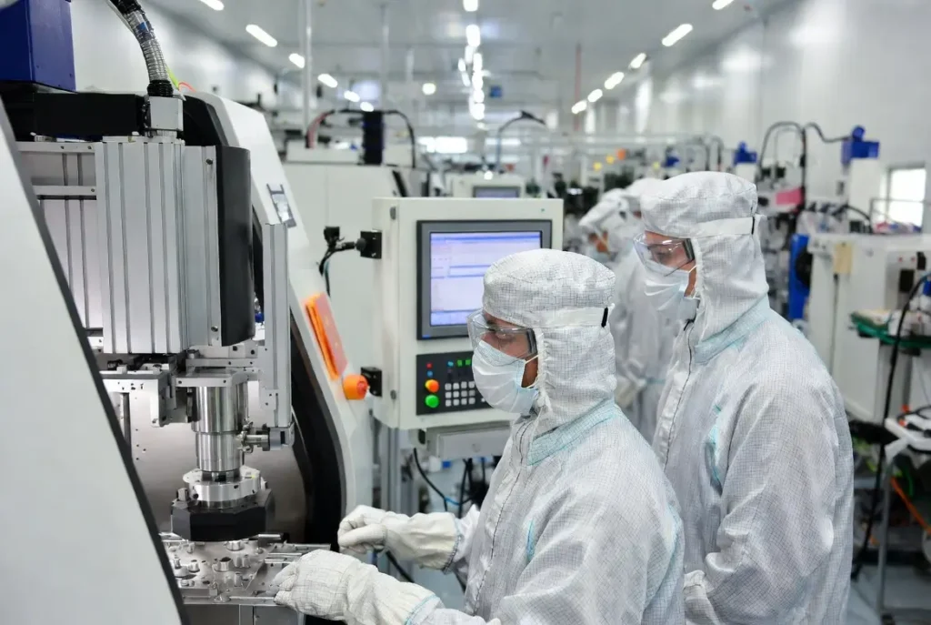
Cleanroom CNC Machining and Contamination Control
Semiconductor fabrication environments operate under extremely strict contamination standards. According to SEMI, particles larger than 0.1 µm can cause catastrophic defects in advanced semiconductor nodes [2].
Sources of contamination introduced by machining include:
- Micro burrs formed during cutting
- Residual particles embedded in surfaces
- Surface roughness leading to particle shedding
- Chemical residues from cutting fluids
Therefore, cleanroom CNC machining must include not only precision manufacturing but also controlled finishing and cleaning processes.
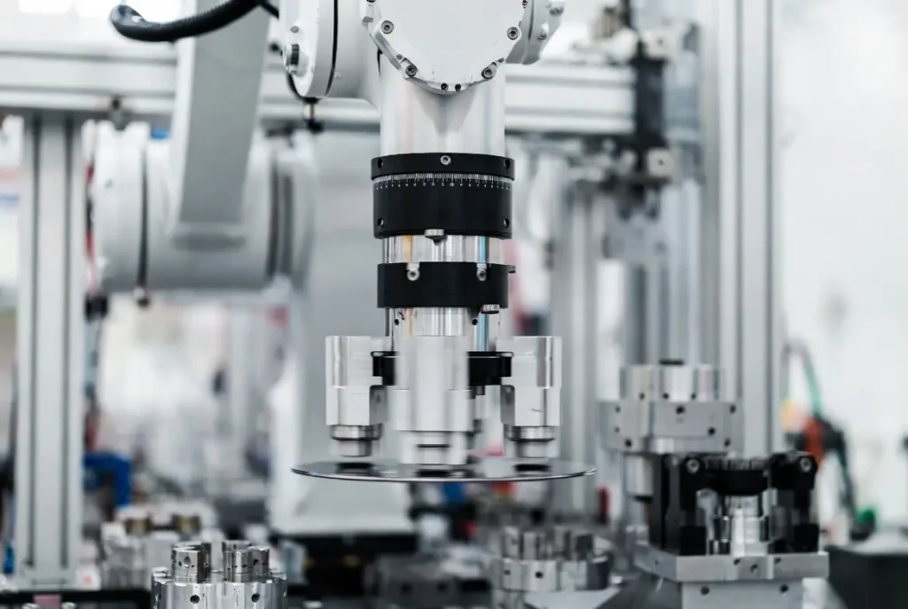
Structural Complexity of Semiconductor Equipment
Modern semiconductor equipment is no longer purely mechanical—it integrates:
- Precision mechatronic systems
- Optical alignment modules
- Vacuum and gas flow systems
- Thermal management structures
CNC machining must support these systems by producing components with:
- Complex geometries
- Tight tolerances
- Multi-functional surfaces
Advanced semiconductor equipment machining relies heavily on 5-axis CNC systems and optimized toolpath algorithms [3].
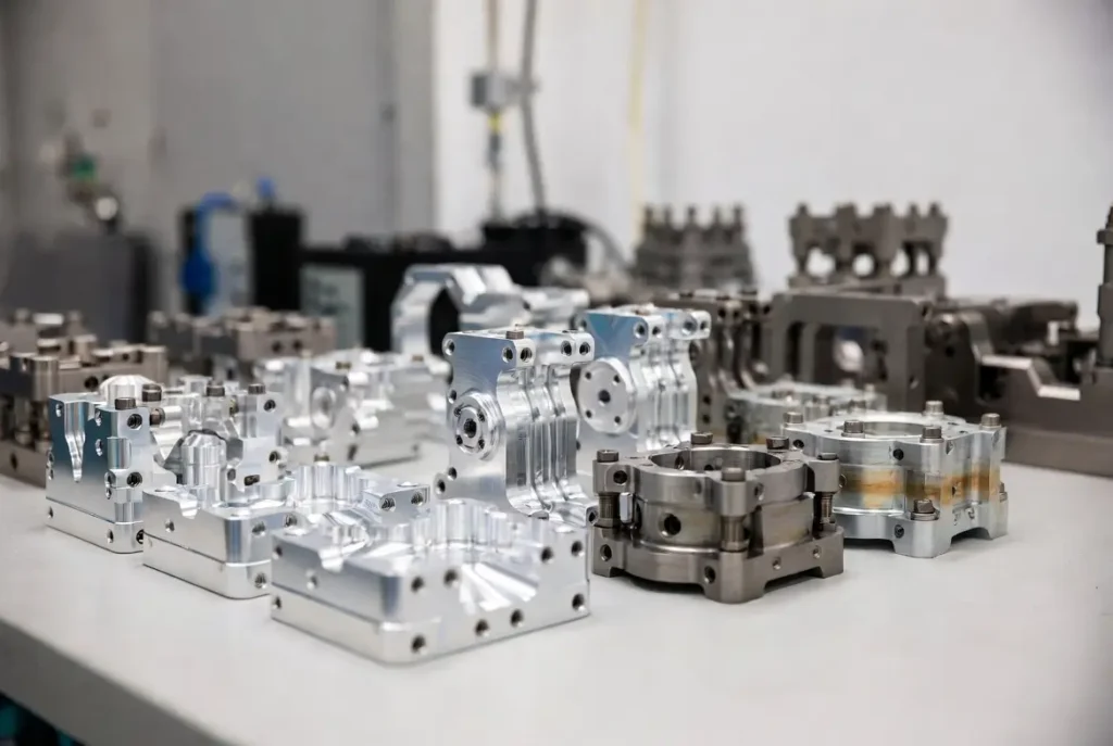
Key Applications of Semiconductor CNC Machining Parts
Wafer Handling Systems
Wafer handling systems are responsible for transporting fragile wafers between process stages.
Key requirements include:
- Positioning accuracy < ±2 µm
- Low vibration and high stiffness
- Minimal particle generation
Even small mechanical deviations can result in wafer misalignment or breakage.
Vacuum Chambers
Vacuum chambers are used in deposition and etching processes and must maintain ultra-high vacuum conditions.
Requirements include:
- Leak rate < 10⁻⁹ mbar·L/s
- Smooth sealing surfaces
- High dimensional stability
CNC machining ensures precise sealing interfaces and structural integrity.
Lithography System Components
Lithography systems operate at nanometer resolution, making mechanical stability critical.
CNC-machined components support:
- Optical alignment systems
- Motion stages
- Structural frames
Machining errors can directly lead to overlay defects and yield loss [4].
Plasma Etching and Deposition Equipment
Components must withstand:
- Plasma bombardment
- Thermal cycling
- Chemical corrosion
This requires both advanced materials and precision machining.
Materials for Semiconductor CNC Machining
Material selection is critical for performance, durability, and contamination control.
Aluminum Alloys
- Excellent machinability
- High thermal conductivity
- Lightweight
Widely used in vacuum chambers and structural components.
Stainless Steel
- Corrosion resistance
- Structural strength
- Vacuum compatibility
Engineering Plastics (PEEK, PTFE)
- Low particle generation
- Chemical resistance
- Electrical insulation
Ceramics
- High hardness
- Thermal stability
- Plasma resistance
Material behavior during machining significantly affects tool wear, surface finish, and dimensional accuracy [1].
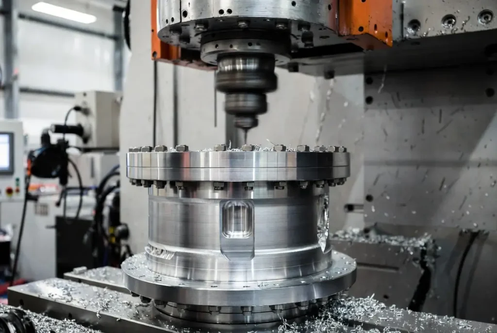
Precision Requirements for Semiconductor Components
Typical requirements for ultra-precision CNC machining include:
- Tolerance: ±1–5 µm
- Surface roughness: Ra < 0.2–0.4 µm
- Flatness: < 2–5 µm
According to NIST, achieving such precision requires advanced metrology, calibration, and uncertainty control systems [6].
Engineering Error Budget in CNC Machining
Machining accuracy is influenced by multiple error sources:
Total Error = Geometric + Thermal + Servo + Tool Wear
Thermal Error Dominance
Thermal deformation accounts for up to 70% of total machining error in precision systems [5].
Sources include:
- Spindle heat
- Cutting heat
- Ambient temperature changes
Servo and Control Errors
Servo errors arise from:
- Position lag
- Interpolation inaccuracies
- Controller limitations
Toolpath planning plays a critical role in minimizing these errors [3].
In simple terms, machining errors mainly come from heat, motion control, and tool wear.
Real Case: CNC Machining Impact on Semiconductor Yield
Case study:
- Required tolerance: ±2 µm
- Actual deviation: 6 µm
Result:
- Wafer misalignment
- Overlay errors
- Yield drop of ~15%
This demonstrates the direct relationship between precision semiconductor components and manufacturing efficiency [4].
Surface Integrity and Functional Performance
Surface integrity includes:
- Surface roughness
- Residual stress
- Microstructure
Poor surface integrity can lead to:
- Seal leakage
- Particle generation
- Reduced fatigue life
Ultra-precision machining aims to minimize subsurface damage and enhance reliability.
Major Challenges in Semiconductor CNC Machining
Burr Formation
At a micro-scale, burr formation is influenced by:
- Tool geometry
- Cutting parameters
- Material properties
Even micro-burrs can become contamination sources [2].
Thermal Deformation
Thermal drift affects machine geometry and must be compensated using:
- Temperature sensors
- Compensation algorithms
- Environmental control [5]
Tool Wear
Tool wear affects:
- Surface roughness
- Dimensional accuracy
Predictive models are used to optimize tool life [1].
Process Stability
Stable machining requires:
- Controlled environment
- Consistent parameters
- Machine calibration
Surface Treatment and Cleanroom Processing
Post-processing ensures cleanroom compatibility:
- Electropolishing
- Anodizing
- Passivation
- Ultrasonic cleaning
These processes remove contaminants and improve surface quality.
CNC Machining vs Other Manufacturing Methods
| Factor | CNC Machining | Injection Molding | Casting |
|---|---|---|---|
| Precision | Ultra-high | Medium | Low |
| Cleanroom suitability | Excellent | Limited | Poor |
| Cost | High | Low | Low |
CNC machining is essential for ultra-precision semiconductor components.
Future Trends in Semiconductor CNC Machining
Ultra Precision and Nano Machining
Advances in machine tool design are enabling nano-scale machining capabilities.
Intelligent Manufacturing Systems
AI-driven systems improve:
- Process control
- Predictive maintenance
- Accuracy
Hybrid Manufacturing
Combining CNC machining with additive manufacturing enables new design possibilities.
FAQs
What is CNC machining used for in semiconductors?
CNC machining is used to produce precision components such as wafer handling systems, vacuum chambers, and structural parts of semiconductor equipment.
Why is precision so important in semiconductor machining?
Because even microscopic errors can affect wafer alignment, leading to reduced yield or defects. [4].
What materials are commonly used?
Aluminum, stainless steel, engineering plastics, and ceramics are widely used depending on the application.
Can CNC meet cleanroom requirements?
Yes, with proper finishing [2].
Expert Insight
CNC machining for semiconductor industry will continue to evolve as device complexity increases. Future competitiveness will depend on ultra precision machining, intelligent systems, and contamination control.
Conclusion
CNC machining is a foundational technology in semiconductor manufacturing, enabling the production of high-precision, contamination-free components.
As semiconductor technology advances, CNC machining must continue to evolve in precision, stability, and process control.
[1] O’Toole, L. et al. (2021). Precision Micro-Milling Process. Springer https://link.springer.com/book/10.1007/978-3-030-72670-7
[2] SEMI Standards https://www.semi.org/en/standards https://www.semi.org/en/standards
[3] Toolpath Interpolation and Smoothing for CNC Machining. Springer https://link.springer.com/article/10.1007/s11633-019-1190-y
[4] IEEE Transactions on Semiconductor Manufacturing. https://ieeexplore.ieee.org/xpl/RecentIssue.jsp?punumber=66
[5] CNC machining & precision engineering research Springer https://link.springer.com/article/10.1007/s12541-025-01318-2
[6] NIST Precision Engineering Guidelines https://www.nist.gov/topics/manufacturing