
Semiconductor
Cooling Plate Manufacturing
CNCPioneer is a precision semiconductor cooling plate specialist and certified China cooling plate factory delivering custom cold plate manufacturing — process equipment liquid-cooled cold plates, ATE thermal control cold plates, laser module cold plates, RF power amplifier cold plates, and wafer chuck cooling platforms with cold plate top face flatness of 0.005mm/300mm, internal coolant channel position accuracy of ±0.050mm, and 100% helium or pressure decay leak testing on every plate.
What Is Semiconductor
Cooling Plate Manufacturing?
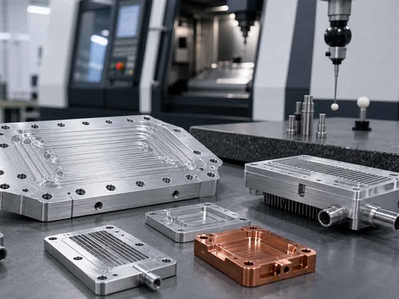
Semiconductor cooling plate manufacturing is the precision CNC machining, surface treatment, leak testing, and cleanliness verification process that produces the liquid-cooled thermal management components constituting the heat extraction infrastructure of semiconductor manufacturing equipment, test systems, and process support equipment.
A semiconductor cooling plate is a precision-machined metallic body — internally channeled for liquid coolant flow — whose external contact surfaces serve as the primary thermal interface between heat-generating semiconductor equipment elements and the cooling system. Unlike industrial cooling plates where ±0.5mm tolerances are adequate, semiconductor cooling plates impose three distinct precision requirements: surface flatness at the thermal contact interface (0.005–0.010mm), coolant compatibility in semiconductor environments (DI water, fluorinated fluids, Galden), and cleanroom/process compatibility (no particle generation, no outgassing).
-
Thermal contact face flatness as the performance foundation At 0.005mm flatness, the TIM layer compresses to uniform 75 ± 3μm bond-line thickness, producing target thermal resistance. At 0.020mm flatness, thermal resistance varies 27%, causing hot spot temperatures 8–15°C above design. CNCPioneer achieves 0.005mm by CBN precision surface grinding with thermal stabilization — verified by 25-point CMM grid on every plate.
-
DI water compatibility as a cleanroom competency DI water is chemically aggressive — it leaches metallic ions from copper (0.1–1.0 ppb/day) and bare aluminum. CNCPioneer's DI water programs specify 316L electropolished stainless or anodized 6061-T6 aluminum with confirmed ion extraction test data. Copper and brass are NOT acceptable for DI water circuits.
-
Fluorinated coolant compatibility for sub-ambient programs Galden HT-135, Fluorinert FC-77, and Novec 7100 require FFKM (Kalrez) or PTFE-encapsulated O-rings — standard nitrile (NBR) seals are attacked. CNCPioneer's fluorinated coolant programs specify correct O-ring groove geometry for Kalrez seals and verify sealing compatibility before manufacturing commitment.
-
40–60% China cooling plate factory cost advantage CNCPioneer delivers 40–60% below equivalent US, European, and Japanese specialist cold plate manufacturers at identical flatness, channel accuracy, leak test documentation, and cleanroom packaging — enabling semiconductor equipment OEMs to achieve BOM cost targets in competitive capital equipment markets.

Why CNCPioneer —
Semiconductor Cooling Plate Manufacturer
Key advantages establishing CNCPioneer as the preferred semiconductor cooling plate and cold plate manufacturing specialist — from thermal contact face flatness and DI water compatibility to precision channel machining, 100% leak testing, and China cooling plate factory economics.
Thermal Contact Face Flatness
At 0.005mm flatness, the TIM layer compresses to uniform 75 ± 3μm bond-line thickness, producing thermal resistance R_th = 0.006 K/W for a 50mm×50mm device — the target value in thermal design. At 0.020mm flatness, BLT varies 75–95μm, producing a 27% thermal resistance range that causes hot spots 8–15°C above design. CNCPioneer achieves 0.005mm by CBN precision surface grinding with thermal stabilization protocol.
DI Water Compatibility
Semiconductor equipment uses deionized water (18 MΩ·cm) as primary coolant. DI water leaches copper ions at 0.1–1.0 ppb/day — contaminating water, depositing on heat exchangers, and potentially reaching wafer surfaces. 316L electropolished stainless (ion leaching ≤0.01 ppb Fe/hour) and anodized 6061-T6 aluminum are the correct materials. CNCPioneer specifies and verifies ion extraction test data before program commitment.
Fluorinated Coolant Compatibility
ATE systems cooling to −40°C to −55°C and laser systems at 15–25°C use Galden HT, Fluorinert FC-77, and Novec 7100. These fluids attack standard nitrile (NBR) O-rings — requiring FFKM (Kalrez) or PTFE-encapsulated seals. CNCPioneer's programs specify correct O-ring groove geometry for Kalrez seals and verify sealing compatibility before manufacturing commitment.
Precision Channel Machining
Semiconductor cooling plates require channel width ±0.050mm (versus ±0.100–0.200mm in industrial cold plates) for controlled hydraulic resistance; channel depth uniformity ±0.030mm for consistent heat transfer coefficient; and inter-channel wall thickness uniformity ±0.030mm for consistent conductive resistance. CNCPioneer achieves this on MAZAK mill-turn centers with solid carbide end mills and through-spindle coolant.
100% Leak Testing with Full Traceability
Coolant leaks in semiconductor equipment are catastrophic. CNCPioneer applies 100% helium leak testing (sensitivity ≤1×10⁻⁸ Pa·m³/s) or pressure decay testing (1.5× rated pressure, 30-second hold, zero decay) on every semiconductor cooling plate, with test results recorded against plate serial number — the traceability documentation that OEM quality systems require.
China Cooling Plate Factory Cost Advantage
CNCPioneer delivers 40–60% below US, European, and Japanese specialist cold plate manufacturers at identical flatness, channel position accuracy, leak test documentation, and cleanroom packaging. The cost advantage enables semiconductor equipment OEMs to achieve BOM cost targets in competitive capital equipment markets — from single prototypes through 100,000+ annual unit volumes.
Semiconductor Cooling Plate
Types We Manufacture
CNCPioneer's semiconductor cooling plate programs cover the complete thermal management component architecture of semiconductor capital equipment — from plasma process chamber electrodes and CVD susceptors through ATE thermal forcing cold plates, laser diode bar cold plates, RF amplifier cold plates, and wafer chuck cooling platforms.

Plasma Process Chamber Electrode Cooling Plates
ICP and CCP etch tools, PECVD reactors, and PVD magnetron sputtering tools require water-cooled lower electrodes and chuck assemblies. Electrode cold plate top face flatness 0.010mm/300mm; coolant channel distribution in radial or spiral serpentine pattern for center-to-edge temperature uniformity (ΔT_wafer ≤2°C); channel pitch ±0.100mm; process chemistry compatibility with F-based or Cl-based gases; DI water or PGW circuits; Ø200–Ø450mm for 200mm–300mm wafer tools.

CVD and ALD Susceptor Cooling Platforms
Chemical vapor deposition and atomic layer deposition processes require precise substrate temperature control. Susceptor mounting face flatness 0.010mm/300mm; annular concentric ring channels for azimuthally symmetric cooling; inner ring flow rate 1.5–2.0× outer ring per design; thermal distortion calculation included in DFM review; 316L stainless for DI water coolant and process-chemistry-resistant exterior.

ATE Thermal Control Cold Plates
Device thermal forcing cold plates for burn-in and test: temperature range −55°C to +175°C; DUT contact face flatness 0.005mm; Ra 0.1μm for direct-contact thermal forcing; heater element integration with cartridge heater bores ±0.020mm; RTD or thermocouple bores ±0.005mm; micro-channel option for highest heat flux programs (channel width 0.5–1.0mm; depth 3–5mm); Galden and fluorinated fluid compatible.

Laser and Photonics Cold Plates
Laser diode bar cold plates: contact surface flatness 0.002–0.003mm for solder-mount programs; Ra 0.05–0.10μm mirror polished; gold or indium plating 1–3μm on CuW or copper; micro-channel geometry 0.2–0.5mm width, 2–4mm depth, 0.1–0.3mm wall; CuW 10/90 CTE-matched to GaAs (6.5 ppm/°C). Solid-state laser pump module cold plates; CO₂ laser RF exciter cold plates; fiber laser pump diode cooling plates.

RF Power Amplifier Cold Plates
RF power generators for semiconductor plasma process tools (13.56 MHz, 27.12 MHz, 60 MHz at 1–30 kW) use LDMOS or GaN RF transistors mounted on precision cold plates. Transistor mounting face flatness 0.005mm; multiple transistor mounting zones co-planar within 0.010mm; microstrip ground plane integration with Ra 0.4μm and gold plate 1–3μm; DI water or PGW at 15–25°C; Galden for precision temperature control ±0.1°C.

Wafer Chuck and ESC Base Cooling Plates
Electrostatic chuck base cooling plates: top face flatness 0.005mm/300mm for dielectric bond; helium backside gas micro-grooves ±0.020mm width, ±0.010mm depth; liquid coolant channels ±0.050mm; HV feedthrough bore ±0.005mm; temperature uniformity ±0.5°C across 300mm wafer. Probe station thermal chuck cold plates: flatness 0.005mm/200mm; vacuum groove for wafer retention; cryogenic 316L option for −65°C programs.
Industries & Applications
CNCPioneer's semiconductor cooling plate manufacturing serves every industry consuming precision liquid-cooled thermal management components at documented dimensional accuracy, cleanroom material compliance, and coolant compatibility verification.

Semiconductor Capital Equipment
Complete semiconductor cooling plate manufacturing programs covering the full cold plate BOM for process equipment platforms — electrode cooling plates for etch and CVD tools; ion implant beam-line cold plates; high-power RF generator cold plates; ESC base cooling plates; and susceptor cooling platforms. Single China cooling plate factory supply relationship for complete thermal management component BOM across platform variants.

ATE System Builders
ATE thermal forcing cold plate manufacturing for device-level temperature cycling test — burn-in cold plates (−55°C to +175°C range); wafer-level thermal chuck cooling platforms; probe station thermal chuck cold plates with vacuum groove networks; and large-format burn-in board cold plates. Galden-compatible and DI water circuit programs with 100% leak test documentation.
Laser Equipment
Laser diode bar cold plates in CuW composite (CTE-matched to GaAs and InP); laser pump module cold plates in 6063-T5 aluminum; solid-state laser power supply cold plates; CO₂ laser RF exciter cold plates; and fiber laser pump diode cooling plates. Gold-plated contact zones for direct-bond programs; ultra-precision grinding to 0.003mm contact face flatness for bare-die solder-mount programs.
RF and Microwave Equipment Producers
RF power amplifier cold plates for semiconductor process equipment plasma generators; GaN transistor cold plates in CuW for 5G semiconductor characterization equipment; RF power divider and combiner cold plates for ATE RF signal distribution; and microwave antenna test equipment cold plates with microstrip ground plane integration.

Semiconductor Power Supply Manufacturers
High-voltage power supply cold plates for ion implant extractor power supplies; DC arc supply cold plates for PVD sputtering; programmable DC supply cold plates for ATE bias supplies; and RF power supply cold plates for plasma tools. IGBT and SiC MOSFET mounting surfaces at 0.005–0.008mm flatness with TIM-mount programs.
Wafer Probe System Developers
Probe station thermal chuck cooling plates with vacuum hold-down groove networks; cryogenic chuck cold plates (316L stainless, −65°C LN₂-cooled programs); and probe card thermal management cold plates for multi-site high-speed device test with precision temperature uniformity ΔT ≤1°C across 300mm wafer diameter.
Semiconductor Cooling Plate
Process & Capabilities
CNCPioneer's semiconductor cooling plate manufacturing runs on 66+ MAZAK mill-turn centers, MAZAK VARIAXIS 5-axis platforms, 78+ Swiss CNC lathes, precision surface grinding systems, and dedicated wire EDM equipment — from single prototype semiconductor cold plates through 100,000+ annual unit volumes.
24-Hour Engineering DFM Review
Thermal resistance calculation confirming channel geometry achieves target R_th at specified flow rate and coolant; minimum channel wall thickness pressure capability (FEA at 3× rated pressure); coolant compatibility analysis (material + surface treatment recommendation for specific coolant type and temperature); residual stress relief protocol specification for long cold plates (>300mm); CTE mismatch analysis for direct-bond cold plate programs; ASTM E595 TML compliance pathway for cleanroom-adjacent programs; leak test protocol selection (pressure decay vs. helium).
MAZAK Mill-Turn Manufacturing
Standard semiconductor cold plate machining sequence on MAZAK mill-turn centers: rough face mill → rough channel mill → port bore rough → residual stress relief (175°C × 3 hours) → finish channel mill (±0.050mm width, ±0.050mm depth) → port finish bore and thread (±0.005mm) → O-ring groove machining (±0.015mm width, ±0.010mm depth) → fitment machining → pressure decay pre-test → precision surface grinding → final cleaning → 100% leak test → final CMM.
Precision Surface Grinding — Contact Face
CBN grinding program for 0.005mm flatness target: CBN 170 grit (coarse) → CBN 280 grit (intermediate) → CBN 600 grit (fine finish). Temperature-controlled coolant at 15°C ±0.5°C prevents plate temperature rise above 25°C. In-process flatness check after each fine-pass sequence with adaptive grinding depth correction. 15-minute thermal equilibration hold at 20°C ±0.5°C before final CMM measurement. 25-point grid measurement with maximum deviation from least-squares reference plane reported.
5-Axis Semiconductor Cold Plate Programs
MAZAK VARIAXIS 5-axis for compound-geometry semiconductor cold plates — curved electrode cooling plates, sector-shaped susceptor cooling platforms, and non-rectangular cold plates with compound mounting interfaces. Curved contact face machining with surface form tolerance ±0.020mm; internal channel following curved manifold through non-uniform wall thickness body; all features from one 5-axis datum reference. Micro-channel cold plates for laser diode bars (channel width 0.2–1.0mm ±0.020mm).
Vacuum Brazing and Diffusion Bonding
Brazed cover plate construction: channel network machined in one body face; precision cover plate (flatness 0.005mm before brazing) brazed to close channels; vacuum furnace brazing at 590–610°C in 10⁻⁵ Torr; post-braze leak test at 2× rated pressure; post-braze precision face grinding restores 0.005mm flatness. Diffusion bonding for copper micro-channel cold plates: 850°C, 20 MPa, 4 hours; copper-to-copper interdiffusion bond; 100% helium leak test ≤1×10⁻⁹ Pa·m³/s.
IATF 16949 / AS9100D Documentation
CMM dimensional report: 25-point flatness grid, channel dimensions, port positions, O-ring groove dimensions. Profilometry: contact face Ra; groove Ra. Pressure decay or He leak test record per plate serial number. Material certification: EN 10204 3.1 or ASTM mill certificate. ASTM E595 TML batch certificate. Plating XRF thickness records (Au/Ni-P programs). PPAP Level 3 for OEM programs. All records retained 20 years.
Materials for Semiconductor
Cooling Plate Manufacturing
Semiconductor cooling plate material selection is governed by thermal conductivity, coolant compatibility, CTE matching for direct-bond devices, cleanroom compliance, and operating temperature range. Aluminum 6061-T6 dominates as the best all-round material for standard programs.
Aluminum 6061-T6
167 W/m·K · 2.70 g/cm³ · CTE 23.6 ppm/°C · The dominant semiconductor cooling plate material — best machinability on MAZAK mill-turn centers, good thermal conductivity, and compatible with Type II anodize and electroless Ni-P for DI water circuits. Used for ATE cold plates, power supply cold plates, process equipment cold plates, and wafer chuck platforms. Standard electrode cooling plate material with Type III hard anodize on plasma-exposed surfaces.
Aluminum 6063-T5
200 W/m·K · 2.70 g/cm³ · CTE 23.5 ppm/°C · Maximum aluminum thermal conductivity for thermal-critical cooling plates — laser pump diode cold plates and RF amplifier cold plates where every additional W/m·K reduces junction temperature. Slightly softer than 6061-T6 but adequate for all non-wear-exposed semiconductor cooling plate applications.
Aluminum 1050A
229 W/m·K · 2.71 g/cm³ · CTE 23.7 ppm/°C · Maximum purity aluminum for minimum ion extraction in ultra-pure DI water circuits. Highest aluminum conductivity available; used when even 6063-T5's 200 W/m·K is insufficient and when ionic contamination must be minimized below 6061-T6 levels.
Stainless 316L
16 W/m·K · 7.99 g/cm³ · CTE 16.0 ppm/°C · Primary material for DI water circuit cold plates — ion leaching rate ≤0.01 ppb Fe/hour at 20°C, negligible contamination. Electropolished to Ra ≤0.2μm for minimum ion leaching. UHV-compatible for ion implant beam-line cooling. Maintains ductility to −196°C for cryogenic programs. Mandatory for DI water circuits above 80°C where Ni-P dissolution risk exists.
Copper C11000 / C10100
391 W/m·K · 8.94 g/cm³ · CTE 17.0 ppm/°C · Maximum thermal conductivity for high-flux cold plates — Faraday cup cooling, electromagnet coil cooling, and laser diode micro-channel cold plates. C10100 OFC (oxygen-free) for UHV-adjacent equipment. Nickel electroless 3μm post-machining for corrosion protection and solder-wettable base. NOT for DI water circuits — Cu²⁺ ion contamination risk.
CuW Composite 10/90 & 15/85
180–200 W/m·K · 16.3–17.0 g/cm³ · CTE 6.5–7.2 ppm/°C · CTE-matched to GaAs (6.0 ppm/°C) and InP (4.6 ppm/°C) for laser diode bar direct-bond cold plates. Gold-plated contact zone 1–3μm; 0.002–0.003mm contact face flatness. CuW 10/90 for GaAs laser bars; CuW 15/85 for InP/GaN wide-bandgap devices. Prevents solder joint fatigue over thermal cycling.
AlSiC & Diamond-Cu
AlSiC: 170–200 W/m·K · 3.0 g/cm³ · CTE 7–8 ppm/°C · Low CTE, lightweight versus CuW for power module cold plates requiring CTE match to SiC ceramics. Diamond-Cu: 400–500 W/m·K · 5.9 g/cm³ · CTE 7.0 ppm/°C · Ultra-high thermal conductivity for highest-flux laser diode and GaN RF transistor direct-bond applications.
Titanium, Invar 36, Others
Ti Grade 2: 17 W/m·K · non-magnetic · non-sparking · for MRI-adjacent cooling plates. Invar 36: 11 W/m·K · CTE 1.6 ppm/°C · minimum thermal expansion for athermal cold plates in precision optical systems. All materials XRF-verified per lot with EN 10204 3.1 or ASTM mill certificates archived.
Surface Treatments for
Semiconductor Cooling Plates
Semiconductor cooling plate surface treatment selection addresses corrosion protection in DI water and fluorinated coolant environments, wear resistance on process-exposed surfaces, electrical isolation requirements, and cleanroom outgassing compliance — with coating allowances machined-in and verified post-treatment.
Type II Clear Anodize — MIL-A-8625
5–15μm clear anodize for standard aluminum semiconductor cooling plates — corrosion protection in PGW and fluorinated coolant environments; electrically insulating outer surface for equipment electrical isolation; ASTM E595 TML ≤0.020% for enclosed equipment programs. Bore allowance: port bores and mounting bores machined with 5–8μm per side anodize growth allowance; post-anodize bore diameter 100% air-gauge verified. Contact face masked during anodize to maintain flatness and Ra.
Type III Hard Anodize — MIL-A-8625
HV 400+ hardness for aluminum semiconductor cold plate surfaces exposed to repeated tool installation, handling contact, or plasma species in electrode cold plate programs. Black hard anodize for thermal emissivity management on radiation-dominant thermal paths in vacuum environments. Contact face must be masked — hard anodize dimensional growth (20–50μm per side) would consume the ±0.005mm flatness tolerance on the thermal contact surface.
Electroless Nickel-Phosphorus — MIL-C-26074
The mandatory surface treatment for aluminum semiconductor cold plates in DI water cooling circuits — 5–8μm thickness provides continuous corrosion barrier preventing aluminum dissolution and Al³⁺ ion contamination. High-P Ni-P (10–12% P) for maximum corrosion resistance and non-magnetic requirement. Dimensional allowance: 5–8μm per side; contact face machined undersize by 10–16μm total before Ni-P; post-Ni-P flatness re-verified. Stable in DI water to 60°C; above 80°C, 316L stainless recommended.
Electropolish — 316L Stainless
For 316L stainless semiconductor cold plates in DI water circuits and UHV-adjacent applications — Ra ≤0.2μm on all coolant-wetted surfaces; ASTM E595 TML ≤0.010%; minimum ion leaching into DI water. CNCPioneer coordinates electropolish through qualified EP partners with 10–20μm per side allowance incorporated in machined dimensions; post-EP dimensional re-verification confirms flatness and bore dimensions within specification.
Gold Plating — Laser Diode Bar Contact
1–3μm hard gold (Au-Co) on Ni 3μm undercoat on CuW or copper laser diode cold plate contact surface — provides solder-wettable base for laser diode bar AuSn or indium solder-mount; low surface resistance at RF current density; stable contact resistance over thermal cycling. XRF thickness verification per cold plate contact zone ±0.2μm. Critical for direct-bond laser diode bar programs where solder fillet uniformity determines device lifetime.
Thermal Spray Coating — Alumina
Alumina (Al₂O₃) thermal spray coating 50–200μm on aluminum electrode cooling plate surfaces — provides electrical isolation between grounded cooling plate and HV or RF-powered electrode while maintaining aluminum body thermal conductance. Coating thermal conductivity ~10 W/m·K; dielectric strength 15–20 kV/mm. Applied post-machining; coating thickness uniformity ±20% per plasma spray process parameters. For plasma process chamber lower electrodes requiring isolation.
All surface treatments on semiconductor cooling plate programs — Type II/III anodize MIL-A-8625, electroless Ni-P MIL-C-26074, electropolish 316L, gold plate ASTM B488, alumina thermal spray, and passivation ASTM A967 — are documented with treatment certifications and post-treatment dimensional verification. Plating and coating allowances are machined-in to dimensions at the CNC machining stage and confirmed post-treatment by air gauge, CMM, or XRF. Treatment selection guidance and dimensional allowance calculation are included in CNCPioneer's 24-hour DFM review.
Quality Assurance for
Semiconductor Cooling Plates
Semiconductor cooling plate quality assurance addresses thermal contact face flatness with 25-point CMM grid verification, coolant channel dimensional accuracy with in-process CMM probing, 100% leak testing with serial-number traceability, and cleanroom packaging per SEMI standard protocols.
Engineering DFM Review
Every semiconductor cooling plate inquiry receives engineering DFM within 24 hours: thermal resistance calculation confirming channel geometry achieves target R_th; minimum wall thickness pressure capability from FEA; coolant compatibility analysis with material and surface treatment recommendation; residual stress relief protocol for long cold plates; CTE mismatch analysis for direct-bond programs; ASTM E595 TML compliance pathway; and leak test protocol selection.
Material & Incoming Verification
SII XRF composition confirmation on every material lot — 6061-T6 (Mg 0.80–1.20%; Si 0.40–0.80%), 6063-T5 (Mg 0.45–0.90%), 316L (C ≤0.030%; Mo 2.0–3.0%), OFC copper (Cu ≥99.99%). Hardness verification T6/T5 condition. EN 10204 3.1 or ASTM mill certificates archived. Surface treatment certification: Ni-P P content 10–12% confirmed by wet chemistry.
In-Process Controls
Wall thickness in-process CMM probe at minimum wall cross-sections during channel machining. Thermal stabilization record per lot (furnace chart with time-temperature trace). Post-stress-relief hardness verification. Pre-grinding leak test on every cold plate before surface grinding investment. Post-grinding thermal equilibration 15 minutes before CMM flatness measurement. SPC Cpk ≥1.67 on face flatness and channel width for volume OEM programs.
Final Inspection — 100% Leak Test
Every semiconductor cooling plate: pressure decay at 1.5× rated pressure (minimum 4.5 bar); NIST-traceable pressure transducer ±0.005 bar; 30-second hold; zero decay acceptance. He leak test (≤1×10⁻⁸ Pa·m³/s) for laser cold plates, DI water 316L plates, and vacuum-adjacent programs. Test date, pressure, duration, result, and technician ID recorded per plate serial number. Failed plates: immediate tag-and-quarantine; root cause CT scan or dye penetrant.
Dimensional & Surface Verification
CMM: 25-point flatness grid, channel positions, port bores, O-ring groove, mounting hole pattern. Profilometry: contact face Ra ≤0.2μm; groove Ra. Thread gauges: GO/NO-GO all port threads. XRF: plating thickness at 3 positions per plated cold plate. Visual under 5×: no chips in channels; no burrs at port entries; no machining marks on contact face. Particle count: 1L DI flush through cold plate at 1L/min; ≤50 particles @0.5μm per liter.
Documentation Package
Certificate of Conformance · CMM dimensional report with 25-point flatness grid · Profilometry Ra records · Pressure decay or He leak test record per serial number · Material certifications with lot traceability · Heat treatment and surface treatment certifications · ASTM E595 TML batch certificate · Plating XRF thickness records · PPAP Level 3 for OEM programs · FAIR per AS9102 for aerospace/defense · Cleanroom packaging per SEMI standard · Records retained 20 years.
IATF 16949 Quality System for
Semiconductor Cooling Plates
CNCPioneer's IATF 16949 and AS9100D certified semiconductor cooling plate quality system addresses the four quality dimensions specific to cold plate manufacturing: thermal contact face flatness governance, coolant channel precision machining, 100% leak testing with serial traceability, and cleanroom compliance documentation.
CBN Precision Grinding — Flatness Structural Guarantee
Contact face flatness 0.005mm/300mm is a structural guarantee delivered by CBN precision surface grinding with thermal stabilization — not an outcome of skilled operators achieving best possible results. CNCPioneer's dedicated grinding systems achieve 0.005mm flatness in production: coarse grind → intermediate grind → fine grind at 0.001mm/pass with temperature-controlled coolant. In-process CMM probe measurement after each fine-pass sequence with adaptive grinding depth correction. 15-minute thermal equilibration before final 25-point CMM grid verification.
- CBN 600 grit fine finish grinding program
- Temperature-controlled coolant at 15°C ±0.5°C
- 25-point CMM grid every plate before release
Channel Precision — In-Process CMM & SPC
Coolant channel width ±0.050mm, depth ±0.050mm, and wall thickness ±0.030mm are maintained by solid carbide end mills with through-spindle coolant on MAZAK mill-turn centers. In-process CMM probe at minimum wall cross-sections during channel machining confirms wall ≥1.5mm before proceeding. SPC control charts on face flatness and channel width with Cpk ≥1.67 for volume OEM programs; adaptive grinding correction when flatness approaches 0.004mm before 0.005mm limit. This precision produces ≤2°C temperature non-uniformity across device array footprints.
- Channel width ±0.050mm production standard
- Wall thickness ±0.030mm in-process verified
- Cpk ≥1.67 on flatness and channel width
100% Leak Test — Serial Number Traceability
Every semiconductor cooling plate receives 100% leak testing: pressure decay at 1.5× rated pressure with NIST-traceable transducer ±0.005 bar, 30-second hold, zero decay acceptance. He leak test (≤1×10⁻⁸ Pa·m³/s) for laser cold plates, DI water 316L plates, and vacuum-adjacent programs. Test results recorded per plate serial number — the traceability documentation semiconductor equipment OEM quality systems require for leak-failure root cause investigation. Failed plates: immediate tag-and-quarantine with CT scan or dye penetrant root cause analysis.
- 100% pressure decay on all cold plates
- He leak test ≤1×10⁻⁸ Pa·m³/s for critical programs
- Test record per serial number archived
PPAP Level 3 & Cleanroom Compliance
PPAP Level 3 qualification for semiconductor equipment OEM supply chains: design records, process flow (including single-setup sequence and stress relief protocol), PFMEA (covering tool wear, channel wall breakthrough, braze joint failure, leak path formation), control plan, MSA on CMM and profilometer measurement systems, initial capability studies (Cpk ≥1.67 on flatness, channel width, and leak test), and part submission warrant. ASTM E595 TML ≤0.020% for anodize programs; ≤0.010% for electropolish 316L. Cleanroom packaging per SEMI standard cleanliness protocols.
- PPAP Level 3 for semiconductor OEM supply
- ASTM E595 TML compliance verified
- Cleanroom packaging per SEMI standards
Semiconductor Cooling Plate Manufacturing FAQ
Common questions from semiconductor capital equipment OEMs, ATE system builders, laser equipment manufacturers, RF equipment producers, and wafer probe system developers about CNCPioneer's semiconductor cooling plate capability, material compatibility, leak testing, and volume production economics.
Deionized water's 18 MΩ·cm resistivity makes it both the ideal semiconductor cooling fluid and an extremely corrosive agent. Copper cold plates — standard in industrial cooling because of copper's 391 W/m·K thermal conductivity — dissolve at measurable rates in DI water. At 25°C in 18 MΩ·cm DI water, copper dissolution produces Cu²⁺ ions at approximately 0.1–1.0 ppb per day per cm². For a typical 300mm×400mm copper cold plate (24,000 mm² wetted surface), daily Cu²⁺ generation is approximately 2,400–24,000 pg/day. These copper ions contaminate the DI water recirculation loop, deposit on heat exchanger surfaces, potentially reach the fab DI water distribution system (where Cu at even 0.1 ppb can deposit on silicon wafers causing carrier lifetime reduction), and cause electrochemical pitting of other metallic components. 316L electropolished stainless steel dissolves at approximately 0.001–0.010 ppb Fe/day per cm² — 10–100× lower than copper. 6061-T6 aluminum with electroless Ni-P coating (10–12% P high-phosphorus variant) provides an intermediate solution: aluminum's 167 W/m·K conductivity is retained, and Ni-P reduces aluminum ion leaching from 50+ ppb/day to <0.1 ppb/day — acceptable for DI water circuit service below 60°C.
Achieving ±0.5°C across a 50mm×50mm DUT footprint requires controlling convective resistance variation (inlet-to-outlet coolant temperature rise) and conductive resistance variation (channel wall thickness uniformity). For convective resistance: limit ΔT_coolant ≤1°C by maintaining mass flow rate ṁ ≥ P_DUT / (c_p × ΔT_max) = 100W / (4,186 × 1) = 0.024 kg/s = 1.4 L/min — achievable with standard port sizes. For a serpentine channel at 5mm pitch (10 parallel passes), each channel carries 0.14 L/min at 0.3 bar pressure drop. For conductive resistance: with 6061-T6 conductivity 167 W/m·K, base thickness 5mm, and channel pitch 5mm, one-dimensional conductive resistance is 1.2 K/W per 25mm² cell. Non-uniform wall thickness ±0.030mm produces ±0.36°C variation per cell — within the ±0.5°C total budget. CNCPioneer's production standard of ±0.050mm channel width and ±0.050mm depth provides 40% tighter tolerance than required, delivering manufacturing margin without unnecessary cost.
Leak test specification depends on the consequence of a leak. Pressure decay testing (CNCPioneer standard for all plates): pressurize with dry air or nitrogen at 1.5× rated pressure, seal, and monitor for 30 seconds. Detection sensitivity for a 1L volume at 6 bar: 0.005 bar drop represents ~1.7×10⁻² Pa·m³/s — adequate for macro-leaks that would produce visible weeping within hours. Adequate for: ATE thermal forcing cold plates, power supply cold plates, and process equipment with secondary containment. Helium leak testing (premium specification): pressurize with helium and detect with mass spectrometer at ≤1×10⁻⁸ Pa·m³/s — 6 orders of magnitude more sensitive. Required for: laser diode bar cold plates (DI water reaching solder-bonded bar causes immediate failure), ESC cooling plates where DI water leaking into vacuum contaminates the process, and ion implant beam-line components where coolant reaching UHV collapses vacuum. CNCPioneer applies pressure decay as standard (100% of plates) and upgrades to helium for critical programs — all results recorded per serial number.
Prototype lead times: standard 6061-T6 ATE cold plate (200mm×250mm, channel machining, Type II anodize, pressure decay) — 8–12 business days; 6063-T5 process equipment cold plate with precision grinding to 0.005mm — 10–14 days; 316L stainless electrode cooling plate (electropolish + He leak) — 10–14 days; 6061-T6 laser module cold plate (0.003mm flatness, gold plated) — 10–14 days; CuW 10/90 laser diode bar cold plate (0.002mm flatness) — 14–18 days; large-format burn-in board 600mm×800mm — 12–16 days. Surface treatment additions: anodize +2–3 days; Ni-P +3–4 days; electropolish +2–3 days; gold plate +3–5 days. Volume economics: a 6061-T6 ATE cold plate costs approximately $320 from a US specialist at 500 units/year; approximately $175 at CNCPioneer prototype; and $68–85 at 2,000 annual units. A 6063-T5 process equipment cold plate (300mm×400mm, 0.005mm flatness, He leak) costs approximately $580 from a US specialist; $320 at prototype; $120–155 at 2,000 units. For an OEM producing 500 tools annually with 4 cold plates per tool at $180 average savings, CNCPioneer delivers $360,000 annual BOM savings.
The flatness of the cold plate contact surface directly determines thermal resistance between the heat-generating device and coolant — governing whether equipment operates within its thermal budget at continuous rated power. For a 50mm×50mm device with K_TIM = 5 W/m·K and target BLT = 75μm: at 0.005mm flatness, BLT varies 75–78μm producing 0.02°C hot-spot above average; at 0.020mm flatness, BLT varies 75–95μm producing 0.16°C hot-spot; at 0.100mm flatness, BLT varies 75–175μm producing 0.80°C hot-spot. For a laser diode bar at 50W/cm², the 0.80°C hot-spot from 0.100mm flatness represents 1.6°C threshold exceedance in a design with 1°C operating margin — causing accelerated laser degradation. CNCPioneer's 0.005mm flatness provides 0.02°C hot-spot, well within all semiconductor equipment thermal margin specifications.
Get a Quote for Semiconductor Cooling Plate Manufacturing
Submit your semiconductor cooling plate drawings, thermal specifications, coolant type, leak test requirement, and annual volume and receive a free thermal engineering DFM review and competitive quotation within 24 hours — covering thermal resistance calculation, channel geometry verification, material and surface treatment recommendation, CTE mismatch analysis, leak test protocol selection, and complete pricing from prototype through volume OEM supply.