
Semiconductor Housings
CNC Turning Services
CNCPioneer manufactures precision semiconductor housings for optical sensors, detectors, vacuum systems, RF shielding and cleanroom equipment. Single-setup CNC turning, Swiss CNC and MAZAK mill-turn machining control bores to ±0.002mm, with ASTM E595 outgassing support and 24-hour DFM review.
Bore-to-bore concentricity reaches ±0.003mm, with face flatness to 0.005mm and Ra 0.4µm on optical contact surfaces. Single-setup machining preserves alignment between optical bores, mounting registers and connector features.
What Are Semiconductor Housings
CNC Turning Services?
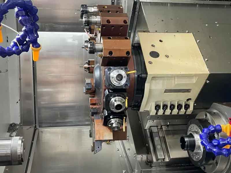
Semiconductor housing CNC turning produces precision enclosure bodies, sensor mounts, detector housings, optical interface tubes and alignment structures for semiconductor equipment, metrology instruments, photonics systems and test platforms.
Unlike general industrial housings, these parts must control coaxiality, contamination, thermal stability, magnetic behavior, EMI shielding and vacuum compatibility. CNCPioneer reviews these requirements during DFM and matches material, machining platform, cleaning and surface treatment to the application.
-
Single-setup coaxial bore machining The most critical geometric relationship in every semiconductor sensor housing is the concentricity between the active element bore and the mounting register bore. CNCPioneer's semiconductor housings CNC turning programs machine both bores in one MAZAK mill-turn chucking from one spindle datum — holding bore-to-bore concentricity at ±0.003mm by machine positioning accuracy rather than chuck re-registration uncertainty (±0.010–0.030mm).
-
Outgassing compliance as material competency ASTM E595 total mass loss (TML) ≤0.05% at 125°C, 24 hours, 5×10⁻⁵ Torr is the standard outgassing specification. Not all aluminum alloys, stainless grades, and surface treatments comply. CNCPioneer's DFM review specifies the correct material + surface treatment combination for each housing's vacuum environment, cleanroom class, and operating temperature.
-
Swiss CNC for miniature housing programs Many semiconductor detector and sensor housings operate at sub-30mm diameter — photodetector module housings Ø8–25mm, laser aperture bodies Ø5–15mm, fiber optic alignment sleeves Ø2–8mm — where L/D ratios and bore tolerances are only achievable on Swiss CNC platforms with guide bushing support. CNCPioneer's 78+ Swiss CNC lathes machine miniature semiconductor housings from Ø1.5mm to Ø30mm.
-
Cleanroom and vacuum-ready support Material selection, machining residue control, surface treatment and ASTM E595 documentation are reviewed for cleanroom, high-vacuum and ultra-high-vacuum programs.

Why CNCPioneer — Semiconductor
Housings CNC Turning Services
CNCPioneer combines single-setup coaxial machining, optical alignment control, ASTM E595 material and finish review, Swiss CNC miniature programs, cleanroom-compatible finishing and one documentation package for semiconductor housing programs.
Single-Setup Coaxial Bore Machining
The most critical geometric relationship in every semiconductor sensor housing is the concentricity between the active element bore and the mounting register bore. CNCPioneer's semiconductor housings CNC turning programs machine both bores in one MAZAK mill-turn chucking from one spindle datum — holding bore-to-bore concentricity at ±0.003mm by machine positioning accuracy rather than chuck re-registration uncertainty (±0.010–0.030mm). This single-setup discipline is not optional for semiconductor housings.
Outgassing Compliance as Material Competency
ASTM E595 total mass loss (TML) ≤0.05% at 125°C, 24 hours, 5×10⁻⁵ Torr is the standard outgassing specification. Not all aluminum alloys, stainless grades, and surface treatments comply — 6061-T6 with Type II clear anodize achieves TML ≤0.02%; machined unprotected surface achieves TML ≈ 0.08% (non-compliant). CNCPioneer's DFM review specifies the correct material + surface treatment combination for each housing's vacuum environment, cleanroom class, and operating temperature.
Swiss CNC for Miniature Housing Programs
Many semiconductor detector and sensor housings operate at sub-30mm diameter — photodetector module housings Ø8–25mm, laser aperture bodies Ø5–15mm, fiber optic alignment sleeves Ø2–8mm — where L/D ratios and bore tolerances required are only achievable on Swiss CNC platforms. CNCPioneer's 78+ Swiss CNC lathes machine miniature semiconductor housings from Ø1.5mm to Ø30mm bar stock at ±0.002mm bore diameter, ±0.001mm roundness, and Ra 0.2μm.
Cleanroom-Compatible Surface Finish Direct from Turning
Ra 0.4μm on aluminum semiconductor housing surfaces is achievable directly from precision CNC turning with PCD insert tooling — eliminating secondary grinding operations that introduce new particulate contamination risks. CNCPioneer's semiconductor housings CNC turning services specify appropriate insert geometry, cutting speed, and feed rate per material to achieve Ra 0.4μm as the direct turning result, verified by profilometry per lot.
Complete Semiconductor Housing Portfolio
Sensor housings, detector enclosures, vacuum interface flanges, optical alignment tubes, encoder housings, and RF shielding bodies — all from CNCPioneer's semiconductor housings custom CNC turning facility under one quality system, one delivery schedule, and one documentation package. From single prototype first articles through 500,000+ annual unit volumes.
Documentation and Production Support
From prototype first article to volume OEM production, programs can include CMM, roundness, profilometry, material certificates, ASTM E595 records, PPAP or FAIR documentation and lot traceability.
Semiconductor Housing Types —
Technical Portfolio
CNCPioneer produces custom housings for optical sensors, detectors, laser modules, vacuum interfaces, wafer handling, encoders, RF shielding and semiconductor test equipment, with turning and mill-turn processes matched to geometry.

Image Sensor and CCD/CMOS Camera Housings
CCD and CMOS image sensor housings are the most geometrically demanding semiconductor housing CNC turning programs — the active element bore, optical window seat, and C/CS-mount or custom lens interface bore must share a common optical axis within ±0.003mm or the imager cannot achieve its designed modulation transfer function (MTF) at full field. Primary bore diameter matched to sensor package OD ±0.002mm; lens mount bore C-mount Ø25.4mm × 32 TPI female thread ±0.005mm pitch diameter; window seat face flatness 0.005mm; Ra 0.4μm on optical contact surfaces. Material: 6061-T6 aluminum standard (Type II clear anodize; ASTM E595 TML ≤0.02%). Standard size range: Ø20mm–Ø120mm OD; bore Ø5mm–Ø80mm; length 10–80mm.

Photodetector and PMT Housings
Photodetector housings for silicon photodiodes, avalanche photodiodes (APDs), and photomultiplier tubes (PMTs) used in spectroscopy, fluorescence measurement, and semiconductor wafer inspection. APD housing: active area aperture bore ±0.005mm diameter; detector package seat ±0.003mm bore for TO-5, TO-8, or TO-18 registration; dark current shielding continuous wall at ≤0.1mm gap; TEC mounting face flatness 0.005mm. PMT housing: PMT tube OD seat ±0.005mm; light entrance aperture precision bore ±0.010mm concentric to PMT tube seat ±0.005mm; mu-metal sleeve seat bore ±0.050mm; HV feedthrough bore ±0.005mm. Material: 6061-T6 or 7075-T6 aluminum (black anodize Type II for internal light scatter suppression); 316L stainless for PMT non-magnetic requirement.

Laser and Light Source Housings
Laser diode module housing: laser diode mount bore ±0.002mm (Swiss CNC) for TO-56, TO-18, or custom package; concentricity to collimating lens bore ±0.003mm — the coaxial relationship governing beam collimation quality and pointing stability. Collimating lens bore ±0.003mm; output beam aperture ±0.010mm concentric to lens bore; thermal management heat sink fin integration on OD or copper insert bore ±0.003mm; TEC interface face flatness 0.005mm; fiber coupling SMA905 or FC/PC connector thread ±0.005mm. DPSS laser housing: crystal mount cavity ±0.010mm; mirror mount bore ±0.005mm; Q-switch aperture ±0.005mm; water cooling channel ±0.100mm with 100% pressure decay leak test at 1.5× rated pressure. Material: 6063-T5 aluminum (200 W/m·K) for maximum thermal management.

Vacuum and Ultra-High Vacuum Semiconductor Housings
Semiconductor process equipment and advanced metrology instruments operate under high vacuum (10⁻⁶ Torr) or ultra-high vacuum (10⁻⁹ Torr). Vacuum flange housing bodies: CF (ConFlat) knife edge Ra 0.1μm on sealing surface; edge profile ±0.020mm; ISO-KF centering ring groove bore ±0.020mm; weld prep geometry ±0.050mm. Wafer handling component housings: end effector blade housing ±0.010mm blade seat; flatness 0.010mm for 300mm wafer compliance; sensor integration pocket ±0.020mm. Material: 6061-T6 hard anodized Type III for particle generation resistance; 316L electropolished for UHV with ASTM E595 TML ≤0.01%.

Optical Alignment Housings
Precision alignment housings for beam steering, beam splitting, and beam shaping elements in semiconductor lithography, inspection, and metrology equipment. Beam splitter cube housing: cube seat bore ±0.005mm; bore angular accuracy ±0.01° for correct 45° incident beam angle; beam input and output ports ±0.003mm coaxial to cube seat bore; port pair perpendicularity ±0.01°. Focusing lens tube: lens bore ±0.003mm; bore tilt ±0.005° governing wavefront error; focus adjustment thread precision lead screw (0.5mm pitch) ±0.003mm pitch diameter for 0.1mm/rev focus travel accuracy. Mirror mount housing: mirror seat bore ±0.003mm; face flatness 0.003mm; flexure adjustment screws M2 or M3 fine thread ±0.003mm pitch diameter; kinematic ball seat ±0.010mm. Material: 6061-T6 or Invar 36 (CTE 1.6 ppm/°C for athermal designs).

Encoder and Position Sensor Housings
Read-head housings for optical encoders, magnetic encoders, and linear position sensors used in semiconductor lithography stages and precision motion control. Optical encoder read-head housing: LED emitter bore ±0.003mm; emitter-to-grating gap ±0.020mm; detector array seat ±0.003mm concentricity to emitter bore; mounting reference face flatness 0.003mm; face perpendicularity to scale direction 0.005mm/100mm. Magnetic encoder read-head: Hall effect IC pocket ±0.005mm from housing reference face for correct magnet-to-IC gap; pole piece bore ±0.005mm for ferrite pole piece. Material: non-magnetic (aluminum, PEEK, or 316L) — magnetic materials would distort the flux pattern from the magnetic scale that the read-head measures.
Industries & Applications
CNCPioneer supports semiconductor equipment OEMs, metrology and inspection builders, photonics and laser manufacturers, vacuum integrators, test-and-measurement teams and precision motion-stage programs.

Semiconductor Manufacturing Equipment OEMs
Custom semiconductor housings CNC turning for lithography, etch, CVD, CMP, and inspection equipment — wafer handling component housings in 6061-T6 hard anodize; vacuum chamber flange bodies in 316L electropolished; laser illumination module housings with integrated thermal management; and sensor integration mounts for in-situ process monitoring equipment.

Semiconductor Metrology and Inspection Instrument
CCD/CMOS image sensor housings for wafer inspection systems; spectrometer detector housings for optical emission spectroscopy; interferometer housing bodies for surface metrology; ellipsometer sensor housings; and AFM scanner housing components — all with ±0.002–0.003mm bore concentricity and ASTM E595 outgassing documentation.

Photonics and Laser Equipment
Laser diode module housings in 6063-T5 for maximum thermal conductivity; fiber-coupled laser housing programs; beam splitter and optical filter housing bodies; PMT and APD detector housings for photon counting instruments; and DPSS laser resonator housing machining programs.

Semiconductor Test and Measurement
RF shielding EMI housing bodies for device characterization; probe station component housings; automated test equipment (ATE) precision interface housings; and burn-in board housing components — Alodine Class 3 EMI bonding surfaces; precision connector feed-through bores ±0.010mm.

Vacuum System Integrators
ConFlat flange housings Ra 0.1μm knife edge; ISO-KF flange bodies; bespoke vacuum chamber port housings; gas delivery manifold housings; and vacuum gauge housing bodies — all in 316L or 304L electropolished stainless with ASTM E595 TML documentation and 100% helium leak test coordination.
Precision Motion and Stage
Encoder read-head housing bodies in non-magnetic materials; linear and rotary position sensor housings; bearing preload housing bodies; and voice coil actuator housing components for semiconductor lithography stage applications — all requiring non-magnetic materials and precision bore-to-reference-face geometric relationships.
Semiconductor Housings CNC Turning
Process Architecture
CNCPioneer's process combines 66+ MAZAK mill-turn centers, 78+ Swiss CNC lathes and 5-axis platforms for single-setup bores, live-tool features, thermal stabilization and documented inspection.
Swiss CNC Turning (Ø1.5–30mm)
Swiss CNC turning with guide bushing support is the mandatory process platform for miniature semiconductor housings where L/D ratios above 3:1 make conventional turning dimensionally non-compliant. Housing OD range Ø1.5–30mm from bar stock; bore diameter accuracy ±0.002mm; bore roundness ±0.001mm; concentricity OD to bore ±0.002mm; surface finish Ra 0.2μm on aluminum optical contact surfaces; complete cycle including OD, bore, face, thread features, O-ring grooves, and connector exit — all in one bar-feed program. TO-can laser diode housing Ø5.6mm × 20mm: complete in 4-minute cycle. Fiber optic ferrule alignment sleeve Ø2.5mm × 10mm: bore Ø1.25mm ±0.001mm; Ra 0.1μm bore.
MAZAK Mill-Turn (Ø30–300mm)
For semiconductor housings above Ø30mm — camera housings, beam splitter cubes, detector modules, and vacuum flange bodies — MAZAK mill-turn single-setup programs combine turning accuracy with C-axis milling. Housing OD range Ø30–300mm; bore accuracy ±0.002mm; concentricity (multi-bore) ±0.003mm; C-axis features (connector exits, mounting holes, cable channels, alignment flats) all from bore datum ±0.005mm position; face flatness 0.005mm; thread accuracy ±0.005mm pitch diameter (C-mount, CS-mount, precision scientific thread interfaces). Thermal stabilization: 20-minute pause after rough boring before finish pass; flood coolant stabilization confirming housing body temperature within 0.5°C of ambient before final bore.
5-Axis CNC (Compound-Geometry Housings)
5-axis simultaneous machining for semiconductor housings with non-orthogonal bore axes, compound-angle optical interfaces, or freeform exterior profiles. Compound-angle bore pairs (beam splitter housings, prism mounts): inter-bore angle accuracy ±0.01° on MAZAK VARIAXIS. Freeform exterior ergonomic profiles: 5-axis simultaneous toolpath at Ra 0.8μm on curved housing surfaces. Non-planar window seat: ±0.005° face tilt machined 5-axis for angled incidence optical window installations. Complete feature integration in single setup eliminating rechucking error from compound-angle relationships.
Thermal Stabilization for Precision
Semiconductor housings with ±0.002–0.003mm tolerances require thermal stabilization between rough and finish operations — cutting heat from rough boring expands a Ø50mm aluminum housing bore by 0.008mm at 7°C localized temperature rise (CTE 23.6 × 7 × 50 = 0.008mm). CNCPioneer's precision semiconductor housing programs include: 20-minute thermal stabilization after rough boring before finish pass; flood coolant stabilization protocol confirming housing body temperature within 0.5°C of ambient before final bore; ambient-temperature CMM verification (not hot-from-machine measurement) confirming bore diameter within ±0.002mm specification at 20°C ± 0.5°C.
In-Process Control & Final Inspection
Single-pass finish bore protocol (one finish pass without tool re-entry) for Ra 0.2–0.4μm achievement. Thermal stabilization documented in process traveler for all ±0.002mm bore programs. In-process air gauge bore measurement after finish bore before part removal. 100% concentricity verification by CMM on all multi-bore semiconductor housings. ASTM E595 batch TML record referenced per surface treatment lot. Final inspection: CMM (Mitutoyo ±0.001mm) all bore diameters, concentricities, face flatness, thread positions, C-axis feature positions; roundness tester; profilometry; thread gauge; eddy current anodize thickness; visual under 10× magnification.
IATF 16949 / AS9100D Documentation
Certificate of Conformance · CMM dimensional report: all bore diameters, concentricity, face flatness, feature positions · Roundness tester: bore roundness, bore cylindricity, OD-to-bore concentricity · Profilometry: bore surface Ra, face surface Ra, external surface Ra · ASTM E595 TML certificate · Thread gauge records · Material certification: EN 10204 3.1 equivalent or ASTM mill certification · PPAP Level 3 for OEM programs: Cpk ≥1.67 on bore diameter and concentricity · FAIR per AS9102 for aerospace and defense programs · All records retained 20 years.
Materials for Semiconductor
Housings CNC Turning
Material selection is based on outgassing, CTE, magnetic behavior, vacuum compatibility and bore machinability; 6061-T6, 316L, Invar 36, Kovar, PEEK and other grades are reviewed per application.
Aluminum 6061-T6
ASTM E595 TML ≤0.02% (anodized) · CTE 23.6 ppm/°C · Best balance of machinability, outgassing compliance, and cost. 6061-T6 aluminum is the default semiconductor housing CNC turning material — outgassing TML ≤0.02% after Type II clear anodize satisfies both cleanroom and HV applications; CTE 23.6 ppm/°C matches common aluminum optical bench systems for athermal alignment; machinability rated "Excellent" enabling Ra 0.2μm surface finish directly from CNC turning without secondary grinding. Standard for camera, sensor, encoder, and vacuum flange housings.
Aluminum 7075-T6
ASTM E595 TML ≤0.02% (anodized) · CTE 23.4 ppm/°C · Highest strength aluminum alloy. Specified for high-stress sensor mounts and stage component housings where 6061-T6's yield strength is insufficient for the mechanical loads. Same outgassing compliance and anodize compatibility as 6061-T6; slightly lower CTE; machinability rated "Good" — requires more frequent tool changes but achieves identical ±0.002mm bore accuracy and Ra 0.4μm surface finish on optical contact surfaces.
Aluminum 6063-T5
ASTM E595 TML ≤0.02% (anodized) · CTE 23.5 ppm/°C · 200 W/m·K thermal conductivity — the highest of common aluminum alloys. Specified for laser diode module housings and thermal management-intensive semiconductor housing programs where heat spreading from laser drivers, TEC hot sides, or power electronics determines housing design. Slightly lower strength than 6061-T6 but superior thermal conductivity; standard for laser thermal management housings and heat sink-integrated housing bodies.
Stainless 316L
ASTM E595 TML ≤0.01% (electropolished) · CTE 16.0 ppm/°C · Non-magnetic; corrosion resistant; UHV compatible. Specified for ultra-high vacuum chamber flanges, PMT housings where external magnetic field must not enter, and chemical-process-adjacent sensor environments. Electropolished to Ra ≤0.2μm achieves TML ≤0.01% — the lowest outgassing of common housing materials. Non-magnetic (μᵣ ≈ 1.003) satisfies magnetic field measurement instrument requirements that ferromagnetic materials would corrupt.
Stainless 304L
ASTM E595 TML ≤0.01% (electropolished) · CTE 17.2 ppm/°C · Non-magnetic; standard UHV material. Slightly lower molybdenum content than 316L; adequate for vacuum housings and cleanroom hardware where the enhanced corrosion resistance of 316L's 2.0–3.0% Mo is not required. Electropolish + vacuum bake at 150°C achieves TML ≤0.01%. Standard passivation ASTM A967 mandatory for all 304L and 316L components.
Stainless 17-4PH H900
ASTM E595 TML ≤0.01% · CTE 10.8 ppm/°C · High strength; corrosion resistant. Martensitic precipitation-hardened stainless steel for high-strength sensor mount and housing structures where 316L's yield strength is insufficient. H900 aging to HRC 44–47 produces 1,310 MPa yield strength — the strength of alloy steel with the corrosion resistance of stainless. Passivation mandatory; electropolish available for UHV programs requiring both strength and lowest outgassing.
Invar 36 (UNS K93600)
ASTM E595 TML ≤0.02% · CTE 1.6 ppm/°C · Athermal optical bench housings; CTE-matched precision stage components. Specified when the semiconductor housing must maintain optical alignment through temperature excursions — its CTE of 1.6 ppm/°C produces only 0.08μm dimensional change per °C in a 50mm housing, versus 1.18μm per °C for 6061-T6 aluminum. For a ±5°C temperature variation in a 50mm optical housing: Invar 36 changes 0.40μm; 6061-T6 changes 5.9μm — a 14.8× difference. Requires PCD tooling at reduced cutting speeds (v_c = 50–80 m/min).
Kovar (UNS K94610)
ASTM E595 TML ≤0.01% · CTE 5.2 ppm/°C · CTE matches glass/ceramic. Specified for semiconductor housings that hermetically seal glass or ceramic windows, feedthroughs, or substrates — Kovar's CTE 5.2 ppm/°C matches borosilicate glass (CTE 3.3 ppm/°C) and aluminum oxide ceramic (CTE 6.5 ppm/°C) closely enough that glass-to-Kovar hermetic seals maintain integrity through −65°C to +150°C temperature cycling. Gold plating (0.5–2.0μm) for hermetic seal cleanliness and solder-ability.
Titanium Ti-6Al-4V
ASTM E595 TML ≤0.01% · CTE 8.6 ppm/°C · Non-magnetic; lightweight; strong. Specified for MRI-adjacent semiconductor measurement equipment and non-magnetic precision mounts where both strength and zero magnetic permeability are required. Non-magnetic (μᵣ ≈ 1.0005) satisfies MRI-compatibility requirements. Lower CTE than aluminum (8.6 vs 23.6 ppm/°C) provides improved thermal stability for precision optical alignment. DLC coating on bearing-interface zones compensates for lower surface hardness.
PEEK (Victrex 450G)
ASTM E595 TML ≤0.03% · CTE 47 ppm/°C · Electrically isolating; chemical resistant. Specified for isolated sensor bodies and chemical process housings where electrical isolation between sensor and housing ground is required, or where aggressive chemical environments (acids, solvents) would attack metal housings. PEEK achieves TML ≤0.03% without surface treatment — inherently low outgassing polymer. Machinable to ±0.002mm bore and OD tolerance with bore Ra 0.4μm from precision fine-boring; no post-machining heat treatment required.
Aluminum MIC-6 Cast
ASTM E595 TML ≤0.02% · CTE 23.6 ppm/°C · Stress-relieved; dimensional stability. Cast aluminum tooling plate material specified for optical bench housings and precision stage components where stress-relieved cast structure provides superior dimensional stability over wrought 6061-T6. The cast structure's uniform grain distribution and stress relief eliminate the residual stresses from rolling and extrusion that can cause slow dimensional drift in precision optical housings over months of temperature cycling.
Copper C11000 ETP
CTE 17.0 ppm/°C · Electrical ground; thermal conductivity. Specified for EMI shielding insert elements and thermal spreader components within semiconductor housings — copper's electrical conductivity provides superior EMI grounding paths, and its thermal conductivity (400 W/m·K) enables heat spreading from concentrated heat sources (laser diodes, power electronics) across housing surfaces. Not used for primary structural housings due to softness and oxidation; typically as insert or plating substrate.
Surface Treatments for
Semiconductor Housings
Semiconductor housings CNC turning surface treatment selection addresses corrosion protection, outgassing compliance, optical performance, EMI shielding continuity, vacuum compatibility, and wear resistance — with coating allowances machined into precision bore dimensions and verified post-treatment.
Type II Clear Anodize — MIL-A-8625
5–10μm clear anodize on 6061-T6 and 6063-T5 aluminum semiconductor housings — corrosion protection with ASTM E595 TML ≤0.02% compliance; electrically insulating (preventing ground loops at housing-to-sensor interfaces); optically neutral (clear color does not interfere with optical alignment). ASTM E595 outgassing certification available per anodize batch for vacuum program documentation. Standard semiconductor housing treatment.
Type II Black Anodize (Internal Optical Surfaces)
Black sulfuric anodize on internal housing surfaces for light scatter suppression in optical sensor and detector housings — Ra 0.8μm matte black surface reduces internal reflectance to <2% at visible wavelengths, preventing stray light contamination of detector measurements. External alignment bores masked during black anodize; post-anodize bore diameter verified ±0.003mm (anodize growth 5–8μm per side incorporated in machined bore dimensions as standard).
Electropolish (Stainless Steel UHV Housings)
Electrochemical material removal on 304L and 316L stainless semiconductor vacuum housings — Ra ≤0.2μm electropolished surface reduces surface area by eliminating micro-asperities, reducing water molecule physisorption sites and chemisorbed gas retention that drive outgassing in HV/UHV semiconductor equipment. ASTM E595 TML ≤0.01% after electropolish + vacuum bake at 150°C. Electropolish removes 10–30μm of surface material — precision bores machined with electropolish allowance; post-electropolish bores verified to ±0.003mm.
Alodine Class 3 — MIL-DTL-5541 (EMI Housings)
Electrically conductive chromate conversion for aluminum EMI shielding semiconductor housings — contact resistance ≤5 mΩ/cm² at housing seam interfaces for EMC bonding continuity. Clear or yellow chromate; ASTM E595 TML compliant. Provides corrosion protection while maintaining electrical conductivity — the combination required for EMI housing seam bonding that Type II anodize (electrically insulating) cannot provide. Critical for RF shielding enclosure bodies in semiconductor test equipment.
Passivation — ASTM A967 (Stainless Housings)
Mandatory for all 316L, 304L, and 17-4PH stainless steel semiconductor housing components — nitric acid or citric acid passivation restoring chromium oxide passive layer at machined surfaces. Zero dimensional change; ASTM E595 compliant after passivation + cleaning. Applied after all machining is complete including cross-holes, grooves, threads, and bores; passivation liquid penetrates all internal features uniformly. Passivation certificates included in standard shipment documentation.
Gold Plating (Kovar and Copper Components)
0.5–2.0μm gold electroplate on Kovar semiconductor housings for hermetic seal cleanliness and solder-ability; on copper EMI shielding elements for oxidation prevention. Gold plating provides ASTM E595 compliant surface; solder-wettable for component attachment. Critical for Kovar hermetic housing programs where glass-to-metal seals require clean, oxide-free surfaces for reliable sealing integrity through −65°C to +150°C temperature cycling.
DLC Coating (Wear Surfaces)
1–3μm DLC (diamond-like carbon) on semiconductor housing bore surfaces in contact with moving elements — wafer handling blade housings, focus adjustment thread engagement surfaces. Ultra-low friction (μ 0.05–0.15) reduces particle generation at sliding contacts; HV 2,000+ hardness protects precision bore dimensions from contact wear. Critical for wafer handling component housings where particle generation at sliding contacts directly affects wafer yield.
Electroless Nickel (Corrosion + Wear)
For semiconductor process equipment housings exposed to process chemistry — electroless Ni-P (10–12% P) on 6061-T6 aluminum housings achieves HV 500 wear resistance and chemical resistance to dilute acids and mild alkalies encountered in semiconductor wet process equipment environments. Uniform deposition thickness on complex geometries including internal bores and threads; post-plate bore air gauge verification confirms dimensional compliance within ±0.003mm of target.
All surface treatments on semiconductor housings CNC turning programs — Type II clear/black anodize MIL-A-8625, electropolish ASTM E595 ≤0.01%, passivation ASTM A967, Alodine Class 3 MIL-DTL-5541, gold plate, DLC, and electroless Ni-P — are documented with treatment certifications and post-treatment dimensional verification in the shipment package. Plating and coating allowances are machined-in to journal and bore dimensions at the CNC turning stage and confirmed post-treatment by air gauge or profilometry.
Quality Assurance for
Semiconductor Housings CNC Turning
Quality assurance covers coaxiality, contamination control, dimensional stability, non-magnetic or EMI requirements and vacuum compatibility, with records matched to the housing program.
Engineering DFM Review (24 Hours)
Every semiconductor housings custom CNC turning inquiry receives engineering DFM covering: bore concentricity chain feasibility (single-setup vs. precision re-chuck analysis); outgassing TML compliance from material + surface treatment combination for the specified vacuum environment; thermal expansion analysis for athermal design housing programs; cleanroom compatibility of machining process residues; anti-reflective surface specification for optical housings; thread standard verification for C-mount, CS-mount, and scientific thread interfaces; and cost optimization from Swiss CNC vs. mill-turn platform selection.
Material Incoming Inspection
SII XRF composition verification on every semiconductor housing material lot — 6061-T6 (Mg 0.80–1.20%, Si 0.40–0.80%), 7075-T6 (Zn 5.1–6.1%), 316L (Mo 2.0–3.0%, C ≤0.030%), Invar 36 (Ni 35.0–37.0%), PEEK (carbon/hydrogen FTIR confirmation). Material certificates (EN 10204 3.1 or equivalent) received, archived, and cross-referenced to housing serial number. Hardness verification post-aging and post-heat-treatment per lot before final bore finishing.
Precision In-Process Controls
Single-pass finish bore protocol (one finish pass without tool re-entry) for Ra 0.2–0.4μm achievement. Thermal stabilization documented in process traveler for all ±0.002mm bore programs. In-process air gauge bore measurement after finish bore before part removal. 100% concentricity verification by CMM on all multi-bore semiconductor housings. ASTM E595 batch TML record referenced per surface treatment lot. Low-force clamping protocol verification on thin-wall programs.
Final Inspection
CMM (Mitutoyo ±0.001mm): all bore diameters, all concentricities, face flatness, thread positions, C-axis feature positions. Roundness tester: bore roundness and cylindricity per housing. Profilometry: bore surface Ra, face Ra, external surface Ra. Thread gauge: GO/NO-GO all precision threads. Eddy current: anodize thickness at precision bore zones. Visual under 10× magnification: no burrs at bore entries; no machining marks on optical seat faces; no surface contamination.
Volume Production & PPAP
PPAP Level 3 for semiconductor housing OEM programs: bore diameter and bore concentricity Cpk ≥1.67 (IATF special characteristics); face flatness and feature positions Cpk ≥1.33; MSA Gage R&R all gauging ≤10% gauge variation; complete PPAP package including dimensional results, PSW, PFMEA, control plan, and process flow. Volume production at 2-week monthly blanket releases with dedicated capacity.
Documentation Package
Certificate of Conformance · CMM report · Roundness tester concentricity records · Profilometry surface finish records · Material certificates with lot traceability · ASTM E595 TML records per surface treatment batch · Thread gauge records · Anodize thickness records · PPAP Level 3 for OEM programs · FAIR per AS9102 for aerospace and defense programs · All records retained 20 years.
Dimensional Specifications & Industry Standards
CNCPioneer's semiconductor housings CNC turning dimensional specifications and industry standards compliance establish the documented precision and vacuum compatibility that semiconductor equipment OEMs require for cleanroom-deployed instrumentation and process equipment.
Dimensional Specifications
Housing bore diameter ±0.002mm (high precision) via air gauge / CMM. Housing bore roundness ±0.001mm via roundness tester. Bore-to-bore concentricity ±0.003mm via CMM. Face flatness (optical seat) 0.005mm via CMM / interferometer. Thread pitch diameter ±0.005mm via thread gauge + CMM. C-mount thread ±0.003mm. Bore angular relationship ±0.01° via CMM (5-axis). Surface finish (bore) Ra 0.2–0.4μm via profilometry.
- Bore diameter ±0.002mm
- Concentricity ±0.003mm
- Face flatness 0.005mm
Vacuum & Cleanroom Standards
ASTM E595 — TML ≤0.05% standard for HV; ≤0.01% for UHV. ISO 14644 — Classification of air cleanliness for semiconductor cleanroom environments. MIL-A-8625 — Anodic coatings for aluminum (Type II clear; Type II black). MIL-DTL-5541 — Chemical conversion coatings (Alodine Class 3) for EMI-bonded aluminum. ASTM A967 — Passivation for stainless steel vacuum and semiconductor housings.
- ASTM E595 TML ≤0.05%
- ISO 14644 cleanroom compliance
- MIL-A-8625 anodize standard
Quality Management Certifications
IATF 16949:2016 — Automotive-grade quality management for semiconductor housing OEM production programs. AS9100D — Aerospace quality for defense-related semiconductor equipment housing programs. ISO 10012:2003 — Measurement management certified. SEMI E1 — SEMI standard for semiconductor equipment mechanical interface specifications. IEC 61000-4 — EMC immunity testing for RF housing design.
- IATF 16949:2016 Certified
- AS9100D Certified
- ISO 10012:2003 Certified
Production Programs & Lead Times
Prototype first article: 3–10 business days (aluminum 3–5 days; 316L stainless 5–7 days; Invar 36 7–10 days; Kovar 8–12 days). Surface treatments: Type II anodize +2 days; electropolish +2 days; passivation +1 day; gold plate +3 days. Volume: 50–500 units −30–45%; 501–2,000 units −45–58%; 2,001–10,000 units −58–66%; 10,001–50,000 units −66–72%; 50,000+ units maximum discount.
- Prototype: 3–12 business days
- PPAP Level 3: 6–8 weeks
- Volume: 2-week monthly releases
Semiconductor Housings CNC Turning Services FAQ
Common questions from semiconductor equipment OEMs and optical, vacuum, metrology and photonics teams comparing housing CNC turning suppliers.
The requirement for single-setup CNC turning in semiconductor optical housings derives from the coaxial geometric chain that governs instrument optical alignment. Consider a typical CCD image sensor housing: the lens mount bore (where the imaging lens registers) and the sensor seat bore (where the image sensor sits) must share a common optical axis within ±0.003mm for the sensor's active area to lie on the lens's designed focal plane without lateral offset. In multi-setup machining — lens mount bore turned in one chuck, part flipped and sensor seat bore turned in a second chuck — the chuck re-registration introduces an eccentricity of ±0.010–0.030mm between the two bore axes. The consequence: the image sensor sits 0.015mm (average) off the lens optical axis. At a lens magnification of 1×, this 0.015mm lateral offset translates directly to 0.015mm of image displacement — the sensor's active area center does not coincide with the optical axis center, producing field distortion across the imaging area that cannot be removed by flat-field correction. For a 10-megapixel sensor with 5μm pixel pitch, 0.015mm offset corresponds to 3 pixel systematic displacement at the field center — affecting all measurement calculations based on pixel coordinates. Single-setup MAZAK mill-turn machining achieves both bores from the same spindle axis datum, with bore-to-bore concentricity governed by machine positioning accuracy (±0.001–0.002mm) rather than re-registration uncertainty — reducing the systematic alignment error to below one pixel for the same 5μm pixel pitch sensor.
ASTM E595 specifies total mass loss (TML) — the percentage of material weight lost when a sample is exposed to 125°C in vacuum (5×10⁻⁵ Torr) for 24 hours. The semiconductor industry threshold of TML ≤0.05% governs material selection for high vacuum semiconductor equipment, cleanroom-deployed instrumentation, and any housing where outgassed species might contaminate optical surfaces, detector windows, or semiconductor wafers. Surface treatment profoundly affects TML compliance: 6061-T6 aluminum with no surface treatment has TML approximately 0.08–0.15% from absorbed machining oils and atmospheric water in surface oxide pores — non-compliant for HV applications. The same 6061-T6 aluminum with Type II clear anodize (10μm) has TML ≤0.02% — the anodize layer seals the aluminum surface pores, preventing oil absorption during machining, and the anodize post-processing (deionized water seal) removes absorbed machining residues. 316L stainless steel electropolished to Ra ≤0.2μm achieves TML ≤0.01% — electropolish removes the surface oxide layer with trapped contaminants and reduces surface area by smoothing micro-asperities where water physisorbs. PEEK (Victrex 450G) achieves TML ≤0.03% — inherently low outgassing polymer without surface treatment required. CNCPioneer's DFM review for semiconductor housings evaluates ASTM E595 compliance from the material + surface treatment + cleaning protocol combination before manufacturing commitment, using published TML data from material suppliers and surface treatment laboratories — ensuring the delivered housing complies with the vacuum environment specification before the customer commits to manufacturing investment.
Athermal optical housing design — keeping optical alignment stable through temperature variations without active temperature control — is an engineering challenge that is governed by the housing material CTE. The requirement: as housing temperature changes by ΔT, the change in bore-to-bore spacing (effective optical path length) must remain below the optical system's depth-of-focus tolerance. For a laser sensor housing with two aligned bores 40mm apart: 6061-T6 aluminum (CTE 23.6 ppm/°C) produces 40 × 0.0000236 × ΔT mm per °C = 0.00094mm per °C of spacing change. At ±10°C temperature excursion: ±0.0094mm (9.4μm) bore spacing change — significant for optical systems with depth-of-focus below 10μm. Invar 36 (CTE 1.6 ppm/°C) produces 40 × 0.0000016 × ΔT = 0.000064mm per °C — less than 0.001mm (1μm) over ±10°C excursion. CNCPioneer's athermal semiconductor housing CNC turning programs in Invar 36 apply specific machining discipline because Invar's work-hardening rate during turning is high — standard carbide tooling and standard cutting speeds produce built-up edge and poor surface finish. CNCPioneer uses sharp-geometry uncoated or PCD tooling at reduced cutting speeds (v_c = 50–80 m/min for Invar versus 300+ m/min for aluminum), with through-coolant preventing work-hardening from heat accumulation, achieving Ra 0.4μm on Invar bores and ±0.003mm bore diameter accuracy — the combination that delivers both athermal dimensional stability and precision optical alignment capability in the finished semiconductor housing.
Get a Quote for Semiconductor Housings CNC Turning Services
Upload your semiconductor housing drawing or CAD model for a 24-hour DFM and quote review. We will assess single-setup feasibility, bore alignment, material and ASTM E595 needs, thermal expansion, surface finish, thread interfaces and the prototype-to-production path.